
Datasheet

TLE7183F
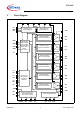
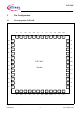
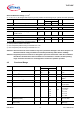
Block Diagram
Data Sheet 4 V2.1, 2008-04-30
2 Block Diagram
Figure 1 Block Diagram
VS
ERR1
ENA1
VDH
ISP
ISN
VTHOC
SH1
GH1
SL1
GL1
SH2
GH2
SL2
GL2
SH3
GH3
SL3
GL3
CL1
Charge Pump 1
Under voltage det.
CH1 CB1 CL2
Charge Pump 2
Under voltage det.
CH2 CB2
Floating HS driver
Short circuit detection
Floating LS driver
Short circuit detection
Floating HS driver
Short circuit detection
Floating LS driver
Short circuit detection
Floating HS driver
Short circuit detection
Floating LS driver
Short circuit detection
L
E
V
E
L
S
H
I
F
T
E
R
Diagnostic logic
Under voltage
Over voltage
Overtemperature
Short circuit
Reset
Over current
INH
ERR1
GND
Current sense OpAmp
Bias reference buffer
Over current warning
VRI VRO VO
Phase voltage feed back
U_fb V_fb W_fb
AGND
IL1
IH1
IL2
IH2
IL3
IH3
Input control
Shoot through
protection
dead time
GND
DT
ENA2
TP