
Datasheet

TLE7183F
Data Sheet 22 V2.1, 2008-04-30
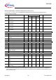
5.3.22 Common mode rejection ratio at
DC
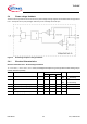
CMRR =
20*Log((Vout_diff/Vin_diff) *
(Vin_CM/Vout_CM))
CMRR 80 100 – db –
5.3.23 Common mode suppression
4)
with
CMS = 20*Log(Vout_CM/Vin_CM)
Freq =100kHz
Freq = 1MHz
Freq = 10MHz
CMS –
62
43
33
– db VIN=360mV*
sin(2*π*freq*t);
Rs=500Ω;
Rfb=7500Ω;
VRI=1.65/2.5V
5.3.24 Slew rate
dV/dt 310–V/µsGain>= 5;
R
L
=1.0kΩ;
C
L
=500pF
5.3.25 Large signal open loop voltage gain
(DC)
A
OL
80 100 – dB –
5.3.26 Unity gain bandwidth GBW 10 20 – MHz R
L
=1kΩ; C
L
=100pF
5.3.27 Phase margin
2)
Φ
M
– 50 – ° Gain>= 5;
R
L
=1kΩ; C
L
=100pF
5.3.28 Gain margin
2)
A
M
–12–dbR
L
=1kΩ; C
L
=100pF
5.3.29 Bandwidth BW
G
1.6 – – MHz Gain=15;
R
L
=1kΩ;
C
L
=500pF;
R
s
=500Ω
5.3.30 Output settle time to 98%
1)
t
set
–11.8µsGain=15;
R
L
=1kΩ;
C
L
=500pF;
0.3<VO< 4.8V;
R
s
=500Ω
5.3.31 Output rise time 10% to 90%
1)
t
Irise
––1µsGain=15;
R
L
=1kΩ;C
L
=500pF;
0.3<VO< 4.8V;
R
s
=500Ω
5.3.32 Output fall time 90% to 10%
1)
t
Ifall
––1µsGain=15;
R
L
=1kΩ;C
L
=500pF;
0.3<VO< 4.8V;
R
s
=500Ω;
1) Input current and output amplifier characteristics:
"Output signal must be amplified and available at 2µs after input signal change (Gain 5...15)
2) Not subject to production test; specified by design
3) calculated out of 5.3.9, 5.3.10, 5.3.11 and 5.3.12
4) Without considering any offsets such as input offset voltage, internal miss match and assuming no tolerance error in
external resistors.
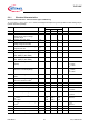
Electrical Characteristics - Current sense signal conditioning (cont’d)
V
S
= 5.5 to 20V, T
j
= -40 to +150°C, F
PWM
< 25kHz, all voltages with respect to ground, positive current flowing into pin
(unless otherwise specified)
Pos. Parameter Symbol Limit Values Unit Conditions
Min. Typ. Max.