
Datasheet

Data Sheet 21 V2.1, 2008-04-30
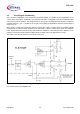
TLE7183F
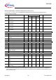
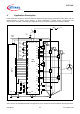
5.3.1 Electrical Characteristics
Electrical Characteristics - Current sense signal conditioning
V
S
= 5.5 to 20V, T
j
= -40 to +150°C, F
PWM
< 25kHz, all voltages with respect to ground, positive current flowing into pin
(unless otherwise specified)
Pos. Parameter Symbol Limit Values Unit Conditions
Min. Typ. Max.
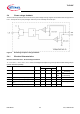
5.3.1 Series resistors
R
S
100 500 1000 Ω –
5.3.2 Feedback resistor
Limited by the output voltage
dynamic range
R
fb
2000 7500 – Ω –
5.3.3 Resistor ratio (gain ratio)
R
fb
/R
S
5–15––
5.3.4 Steady state differential input
voltage range across VIN
1)
V
IN(ss)
-400 – 400 mV –
5.3.5 Transient differential input voltage
range across VIN
V
IN(tr)
-800 – 800 mV –
5.3.6 Input differential voltage (ISP - ISN)
V
IDR
-800 – 800 mV –
5.3.7 Input voltage (Both Inputs - GND)
(ISP - GND) or (ISN -GND)
V
LL
-800 – 1500 mV Vs=5.5..8V
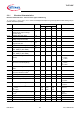
5.3.8 Input voltage (Both Inputs - GND)
(ISP - GND) or (ISN -GND)
V
LL
-800 – 2000 mV Vs=8..20V
5.3.9 Input offset voltage of the I-DC link
OpAmp
V
IO
–1+/-5mVR
S
=500Ω; V
CM
=0V;
V
O
=1.65V;
V
RI
=1.65V
5.3.10 Input offset voltage temperature
drift of the I-DC link OpAmp
2)
V
IO
–12mVR
S
=500Ω; V
CM
=0V;
V
O
=1.65V;
V
RI
=1.65V
5.3.11 Input offset voltage of the reference
buffer
V
IO
1+/-5mV–
5.3.12 Input offset voltage temperature
drift of the reference buffer
2)
V
IO
12mV–
5.3.13 Input range at VRI
V
IO
1.2 – 2.8 V –
5.3.14 Input bias current (ISx to GND)
I
IB
––300µAV
CM
=0V; V
O
=open
5.3.15 High level output voltage of VO
V
OH
4.8 – 5.2 V V
RI
=1.65V/2.5V;
I
OH
=-3mA
5.3.16 Low level output voltage of VO
V
OL
-0.1 – 0.2 V V
RI
=1.65V/2.5V;
I
OH
=3mA
5.3.17 Output voltage of VO
3)
V
RI
= 2.5V,
V
RI
=1.65V
V
OR
2.42
1.58
2.50
1.65
2.58
1.73
VV
IN(SS)
=0V;
Gain=15;
5.3.18 Temperature drift of output voltage
of VO
3)
V
O
0–32mVV
IN(SS)
=0V;
Gain=15
5.3.19 Output short circuit current
I
SC
5––mA–
5.3.20 Differential input resistance
2)
R
I
100––kΩ –
5.3.21 Common mode input capacitance
2)
C
CM
––10pF10kHz