
Datasheet
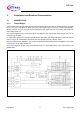

TLE7183F
Description and Electrical Characteristics
Data Sheet 14 V2.1, 2008-04-30
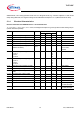
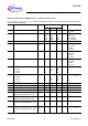
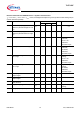
Electrical Characteristics MOSFET drivers - Dynamic Characteristics
V
S
= 5.5 to 20V, T
j
= -40 to +150°C, F
PWM
< 25kHz, all voltages with respect to ground, positive current flowing into pin
(unless otherwise specified)
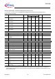
Pos. Parameter Symbol Limit Values Unit Conditions
Min. Typ. Max.
5.1.18 Min. internal dead time
t
DT_MIN
50 – 200 ns DT pin to GND
(R
DT
=0Ω)
5.1.19 Programmable internal dead time
t
DT
0.26
0.64
1.07
2.02
0.41
1.05
1.85
3.82
0.56
1.45
2.63
5.62
µs R
DT
=10 kΩ
R
DT
=47 kΩ
R
DT
=100 kΩ
R
DT
=1000 kΩ
5.1.20 Max. internal dead time
t
DT_MAX
2.33 – 6.35 µs DT pin open
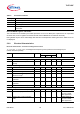
5.1.21 Turn on current, peak
I
G(on)
– 0.8 – A VGxx-VSxx=0V;
Vs=5.5..8V;
C=22nF;
R
Load
=1Ω
5.1.22 Turn on current, peak
I
G(on)
– 1.5 – A VGxx-VSxx=0V;
Vs=8..20V
C=22nF;
R
Load
=1Ω
5.1.23 Turn off current, peak
I
G(off)
– 1.5 – A VGxx-VSxx=10V;
Vs=8..20V
C=22nF;
R
Load
=1Ω
5.1.24 Rise time (20-80%)
T
j
= -40°C
T
j
= 25°C
T
j
= 150°C
t
G_rise
–
150
400
400
700
ns C=22nF; R
Load
=1Ω
5.1.25 Fall time (20-80%)
T
j
= -40°C
T
j
= 25°C
T
j
= 150°C
t
G_fall
–
150
230
230
500
ns C=22nF; R
Load
=1Ω
5.1.26 Input propagation time (low on)
t
P(ILN)
90 190 290 ns C=22nF; R
Load
=1Ω
5.1.27 Input propagation time (low off)
t
P(ILF)
0 100 200 ns C=22nF; R
Load
=1Ω
5.1.28 Input propagation time (high on)
t
P(IHN)
90 190 290 ns C=22nF; R
Load
=1Ω
5.1.29 Input propagation time (high off)
t
P(IHF)
0 100 200 ns C=22nF; R
Load
=1Ω
5.1.30 Absolute input propagation time
difference (all channels turn on)
t
P(an)
––70nsC=22nF; R
Load
=1Ω
5.1.31 Absolute input propagation time
difference (all channels turn off)
t
P(af)
––50nsC=22nF; R
Load
=1Ω
5.1.32 Absolute input propagation time
difference (1channel high off - low
on)
t
P(1hfln)
– – 150 ns C=22nF; R
Load
=1Ω
5.1.33 Absolute input propagation time
difference (1channel low off - high
on)
t
P(1lfhn)
– – 150 ns C=22nF; R
Load
=1Ω