
Datasheet

Data Sheet 13 V2.1, 2008-04-30
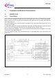
TLE7183F
Description and Electrical Characteristics
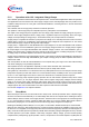
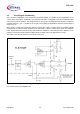
withstand both, +25 V during operation mode and -V
BAT
during INH mode, e.g. a ceramic capacitor. In case of load
dump during INH mode, the negative voltage across CB2 will be clamped to -31 V (CB2 referenced to VDH).
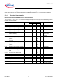
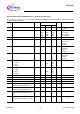
5.1.4 Electrical Characteristics
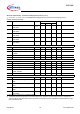
Electrical Characteristics MOSFET drivers - DC Characteristics
V
S
= 5.5 to 20V, T
j
= -40 to +150°C, F
PWM
< 25kHz, all voltages with respect to ground, positive current flowing into pin
(unless otherwise specified)
Pos. Parameter Symbol Limit Values Unit Conditions
Min. Typ. Max.
5.1.1 Low level output voltage
V
G_LL
––0.2VI=30mA
5.1.2 High level output voltage, Low Side
V
G_HL
7.5 – 13 V I=-2mA; Vs=5.5..8V
5.1.3 High level output voltage, High Side
V
G_HL
6.5 – 13 V I=-2mA; Vs=5.5..8V
5.1.4 High level output voltage
V
G_HL
9 – 13 V I=-2mA; Vs=8..20V
5.1.5 High level output voltage difference
dV
G_H
– – 1.0 V I=-100mA; Vs=20V
5.1.6 Gate drive output voltage (device
disabled via ENAx)
V
G(DIS)
– – 0.2 V Disabled;
Vs=5.5..20V;
I=10mA
5.1.7 Gate drive output voltage
Tj=-40°C
Tj=25°C
Tj=150°C
V
G_5
––
1.4
1.2
1.0
V UVLO; Vs<=5.5V
5.1.8 Gate drive output voltage high side
Tj=-40°C
Tj=25°C
Tj=150°C
V
G_HS
––
1.4
1.2
1.0
VOvervoltage
5.1.9 Gate drive output voltage low side
V
G_LS
––0.2VOvervoltage
5.1.10 Low level input voltage of Ixx, ENAx
V
I_LL
––1.0V–
5.1.11 High level input voltage of Ixx,
ENAx
V
I_HL
2.0––V–
5.1.12 Low level input voltage of INH
V
I_LL
––0.75V–
5.1.13 High level input voltage of INH
V
I_HL
2.1––V–
5.1.14 Input hysteresis of IHx, ILx, ENAx
dV
I
50 – – mV Vs=5.5..8V
5.1.15 Input hysteresis of IHx, ILx, ENAx
dV
I
100 200 –- mV Vs=8..20V
5.1.16 Output bias current SHx
I
SHx
0.3 1.0 1.6 mA VSHx=0..(Vs+1);
ILx=low; IHx=high
5.1.17 Output bias current SLx
I
SLx
0.3 1.0 1.6 mA VSLx=0..7V;
ILx=low; IHx=high