
Datasheet

TLE7183F
General Product Characteristics
Data Sheet 10 V2.1, 2008-04-30
Note: Within the functional range the IC operates as described in the circuit description. The electrical
characteristics are specified within the conditions given in the related electrical characteristics table.
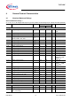
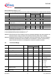
4.3 Default State of Inputs
Table 1 Default State of Inputs
Note: The load condition “C=22nF; R
Load
=1
Ω
” in the paragraph “Electrical characteristics / Dynamic charactersitic” means that
R
Load
is connected between the output Gxx and the positive terminal of the C. The negative terminal of the C is connected
to GND and the corresponding Sxx. The voltage is measured at the positive terminal of the C.
4.2.9 Voltage difference CB2-VDH V
CB2
-0.3 25 V Operation mode
4.2.10 Junction temperature
T
j
-40 150 °C
1) max ratings for Tj has to be considered as well
2) For proper start up minimum Vs=6.5V is required
3) Duty cycle is referred to the high side input command (IHx); The duty cycles can be driven continuously and fully operational
4) total current consumption from power net (Vs and VDH)
Pos. Parameter Symbol Limit Values Unit Conditions
Min. Max.
Characteristic State Remark
Default state of ILx (if ILx left open) Low Low side MOSFETs off
Default state of IHx (if IHx left open) High High side MOSFETs off
Default state of ENA (if ENA1 left open) Low Device outputs disabled
Default state of ENA (if ENA2 left open) Low Device outputs disabled
Default state of INH (if INH left open) Low Sleep mode, I
Q
< 30 µA
Default State of sense amplifier output V
O
(ISP=ISN=0V)
Zero ampere equivalent –
Status of the device and the outputs when
ENA1=ENA2=INH='1'
Device active and outputs functional Vs=5.5..28V
Pull up or pull down integrated resistors
Ixx, ENA
30k
Ω
+/-40% –
Pull down integrated resistor INH 45k
Ω
+/-40% –