
Datasheet


Data Sheet 4 Rev. 2.1, 2007-08-09
TLE6254-3G
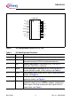
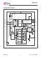
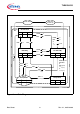
Figure 1 Pin Configuration PG-DSO-14 (top view)
Table 1 Pin Definitions and Functions
Pin No. Symbol Function
1INHInhibit output; for controlling an external voltage regulator
2TxDTransmit data input; integrated pull-up, LOW: bus
becomes dominant, HIGH: bus becomes recessive
3RxDReceive data output; integrated pull-up, LOW: bus is
dominant, HIGH: bus is recessive
4NERRError flag output; integrated pull-up, LOW: bus error (in
normal operation mode), further functions see Table 2
5NSTBNot stand-by input; digital control input to select operation
modes, see Figure 4
6ENTEnable transfer input; digital control input to select
operation modes, see Figure 4
7WKWake-Up input; if level of
V
WAKE
changes the device
indicates a wake-up from low power mode by switching the
RxD outputs LOW and switching the INH output HIGH (in
sleep mode), see Table 2
AEP03323N.VSD
7
6
5
4
3
2
1INH
TxD
RxD
NERR
NSTB
ENT
WK 8
9
10
11
12
13
14
GND
CANL
CANH
RTL
RTH
V
S
V
CC
TLE6254 -3G