
Datasheet


Data Sheet 16 Rev. 2.1, 2007-08-09
TLE6254-3G
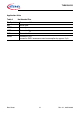
Transmission Input TxD, not Stand-By NSTB and Enable Transfer ENT
HIGH level input voltage
V
IH
0.7 ×
V
CC
– V
CC
+
0.3
V–
LOW level input voltage
V
IL
-0.3 – 0.3 ×
V
CC
V–
HIGH level input current
(pins NSTB and ENT)
I
IH
–2080µA V
i
= 4 V
LOW level input current
(pins NSTB and ENT)
I
IL
0.7 6 – µA V
i
= 1 V
HIGH level input current
(pin TxD)
I
IH
-150 -30 -5 µA V
i
= 4 V
LOW level input current
(pin TxD)
I
IL
-600 -300 -40 µA V
i
= 1 V
Forced battery voltage
stand-by mode (fail safe)
V
CC
2.75 – 4.5 V –
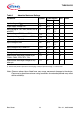
Wake-up Input WAKE
Input current I
IL
-3 -2 -1 µA V
WK
= 0 V
Wake-up threshold
voltage
V
WK(min)
2.2 3.0 3.9 V V
NSTB
= 0 V
Inhibit Output INH
HIGH level voltage drop
∆
V
H
= V
S
- V
INH
∆V
H
–0.10.8VI
INH
= -0.18 mA
Leakage current
I
INH,lk
-5.0 – 5.0 µA sleep operation
mode;
V
INH
= 0 V
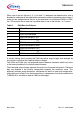
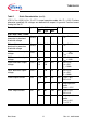
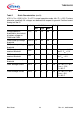
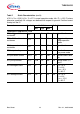
Table 7 Static Characteristics (cont’d)
4.75 V ≤ V
CC
≤ 5.25 V; 6 V ≤ V
S
≤ 27 V; normal operation mode; -40 ≤ T
j
≤ +125 °C (unless
otherwise specified). All voltages are defined with respect to ground. Positive current
flowing into the IC.
Parameter Symbol Limit Values Unit Notes
Min. Typ. Max.