
Datasheet


TLE6254-3G
Data Sheet 13 Rev. 2.1, 2007-08-09
Note: Stresses above those listed here may cause permanent damage to the device.
Exposure to absolute maximum rating conditions for extended periods may affect
device reliability.
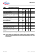
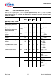
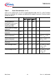
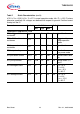
Table 5 Absolute Maximum Ratings
Parameter Symbol Limit Values Unit Notes
Min. Max.
Input voltage at
V
BAT
V
S
-0.3 40 V –
Logic supply voltage
V
CC
V
CC
-0.3 6 V –
Input voltage at TxD, RxD, NERR, NSTB
and ENT
V
IN
-0.3 V
CC
+
0.3
V–
Input voltage at CANH and CANL
V
BUS
-40 40 V –
Transient voltage at CANH and CANL
V
BUS
-150 100 V
1)
Input voltage at WAKE V
WK
-40 40 V –
Input voltage at INH
V
INH
-0.3 V
BAT
+
0.3
V–
Input voltage at RTH and RTL
V
RTH/L
-0.3 40 V –
Junction temperature
T
j
-40 160 °C–
Storage temperature
T
stg
-55 155 °C–
Electrostatic discharge voltage at pin
CANH, CANL, RTH, RTL,
V
BAT
V
esd
-4 4 kV
2)
Electrostatic discharge voltage at any
other pin
V
esd
-2 2 kV
2)
1) See ISO 7637
2) Human body model: equivalent to discharging a 100 pF capacitor through a 1.5 kΩ resistor.