Data Sheet, Rev. 2.1, Aug.
Edition 2007-08-09 Published by Infineon Technologies AG 81726 Munich, Germany © 2005 Infineon Technologies AG All Rights Reserved. Legal Disclaimer The information given in this document shall in no event be regarded as a guarantee of conditions or characteristics.
Fault Tolerant Low Speed CAN-Transceiver TLE6254-3G Features • • • • • • • • • • • • • • • Data transmission rate up to 125 kBaud Low current consumption in stand-by and sleep operation mode, including BUS wake-up Implemented receive-only mode Optimized EMC behavior Wake-up input pin, dual edge sensitive Battery fail flag Extended bus failure management to guarantee safe operation during all bus line failure events Support of failure conditions Fully wake-up capability during all bus line failures condit
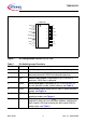
TLE6254-3G T L E6254 -3G IN H 1 14 VS T xD 2 13 GN D R xD 3 12 C AN L N ER R 4 11 C AN H N ST B 5 10 VCC EN T 6 9 RTL WK 7 8 RTH AEP03323N.VSD Figure 1 Pin Configuration PG-DSO-14 (top view) Table 1 Pin Definitions and Functions Pin No.
TLE6254-3G Table 1 Pin Definitions and Functions (cont’d) Pin No.
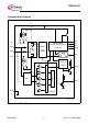
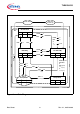
TLE6254-3G Functional Block Diagram VCC VS 14 10 1 RTL CANH CANL 9 7 Mode Control (normal, stand-by, sleep) 11 Driver Output Stage 12 6 5 Time Out WK ENT NSTB TempProtection 2 RTH INH 8 TxD VCC Bus Failure Wake-Up VBat 7.2 Fail Flag 4 NERR -2.8 Filter 3.2 VCC Multiplexer Failure Management 1.8 3 RxD 7.2 GND 13 Receiver AEA03314.VSD Figure 2 Data Sheet Block Diagram 6 Rev. 2.
TLE6254-3G Circuit Description The CAN transceiver TLE6254-3G works as the interface between the CAN protocol controller and the physical CAN bus-lines. Figure 3 shows the principle configuration of a CAN network. The TLE6254-3G is optimized for low-speed data transmission (up to 125 kBaud) in automotive and industrial applications. In normal operation mode a differential signal is transmitted/received.
TLE6254-3G Start Up Power Up Power Down Normal Mode NSTB ENT INH 1 1 High ENT 0 ENT 0 INH 0 High 1 NSTB 0 or VCC Low NSTB 1 NSTB 0 ENT or 0 VCC Low VBat Stand-By NSTB ENT INH 0 0 High NSTB ENT 1 1 1 RxD-Only NSTB NSTB ENT NSTB 0 ENT 1 ENT Wake-Up via CAN-Bus or WK-Input; t > tWU(min) or t > tWK(min) 1 0 ENT t < th(min) Go to Sleep Mode NSTB 0 ENT 1 ENT = 1 t > th(min) INH High Sleep Mode NSTB ENT INH 0 0 Float. AEA03317.
TLE6254-3G Operation Modes, Wake-Up In addition to the normal operation mode, the TLE6254-3G offers a receive-only mode as well as two low power operation modes to save power during periods that do not require communication on the CAN bus: sleep mode, VBAT stand-by mode (see Table 2 and Figure 4). Via the control input pins NSTB and ENT the operation modes are selected by the microcontroller. In the low power modes neither receiving nor transmitting of messages is possible.
TLE6254-3G If either of the supply voltages drops below the specified limits, the transceiver is automatically switched to VBAT stand-by mode or power down mode respectively.
TLE6254-3G When one of the bus failures 3, 5, 6, 6a and 7 is detected, the defective bus wire is disabled by switching off the affected bus termination and the respective output stage. A wake-up from sleep mode via the bus is possible either via a dominant CANH or CANL line. This ensures that a wake-up is possible even if one of the failures 1 to 7 occurs.
TLE6254-3G Application Hints Table 4 Not Needed Pins Pin Symbol Recommendation INH Leave open NERR Leave open NSTB Connect to VCC ENT Connect to VCC WAKE Connect to VBAT, connect to GND: increases current consumption by approx. 5 µA Data Sheet 12 Rev. 2.
TLE6254-3G Table 5 Absolute Maximum Ratings Parameter Symbol Limit Values Min. VS VCC Input voltage at TxD, RxD, NERR, NSTB VIN Unit Notes Max. Input voltage at VBAT -0.3 40 V – Logic supply voltage VCC -0.3 6 V – -0.3 VCC + V – 0.3 and ENT Input voltage at CANH and CANL Transient voltage at CANH and CANL Input voltage at WAKE Input voltage at INH VBUS VBUS VWK VINH -40 40 V – -150 100 V 1) -40 40 V – -0.3 VBAT + V – 0.
TLE6254-3G Table 6 Operating Range Parameter Logic input voltage Battery input voltage Termination resistances at RTL and RTH Junction temperature Symbol Limit Values Unit Notes 5.25 V – 27 V – 0.5 16 kΩ – Tj -40 150 °C – Rthja – 120 K/W – TjSH 160 200 °C 10 °C hyst. VWK -0.3 27 V – Min. Max. VCC VS RRTL/H 4.75 5.
TLE6254-3G Table 7 Static Characteristics 4.75 V ≤ VCC ≤ 5.25 V; 6 V ≤ VS ≤ 27 V; normal operation mode; -40 ≤ Tj ≤ +125 °C (unless otherwise specified). All voltages are defined with respect to ground. Positive current flowing into the IC. Parameter Symbol Limit Values Unit Notes Min. Typ. Max. – 3.5 10.0 mA recessive; TxD = VCC – 6.5 10 mA dominant; TxD = 0 V; no load Supplies VCC, VS Supply current ICC Supply current (Receive-only mode) ICC – 3.5 10.
TLE6254-3G Table 7 Static Characteristics (cont’d) 4.75 V ≤ VCC ≤ 5.25 V; 6 V ≤ VS ≤ 27 V; normal operation mode; -40 ≤ Tj ≤ +125 °C (unless otherwise specified). All voltages are defined with respect to ground. Positive current flowing into the IC. Parameter Symbol Limit Values Min. Typ. Unit Notes Max. Transmission Input TxD, not Stand-By NSTB and Enable Transfer ENT HIGH level input voltage VIH 0.7 × – VCC LOW level input voltage VIL -0.3 VCC + V – 0.3 – 0.
TLE6254-3G Table 7 Static Characteristics (cont’d) 4.75 V ≤ VCC ≤ 5.25 V; 6 V ≤ VS ≤ 27 V; normal operation mode; -40 ≤ Tj ≤ +125 °C (unless otherwise specified). All voltages are defined with respect to ground. Positive current flowing into the IC. Parameter Symbol Limit Values Min. Typ. Max. Unit Notes Bus Lines CANL, CANH Differential receiver recessive-to-dominant threshold voltage VdRxD(rd) -3.6 -3.1 -2.6 V VCC = 5.
TLE6254-3G Table 7 Static Characteristics (cont’d) 4.75 V ≤ VCC ≤ 5.25 V; 6 V ≤ VS ≤ 27 V; normal operation mode; -40 ≤ Tj ≤ +125 °C (unless otherwise specified). All voltages are defined with respect to ground. Positive current flowing into the IC. Parameter Symbol Limit Values Unit Notes Min. Typ. Max. 6.5 7.3 8.0 V – CANH wake-up voltage threshold VCANH,wu 1.1 2.2 2.5 V – CANL wake-up voltage threshold VCANL,wu 2.5 3.1 3.9 V – CANH single-ended receiver threshold VCANH 1.
TLE6254-3G Table 7 Static Characteristics (cont’d) 4.75 V ≤ VCC ≤ 5.25 V; 6 V ≤ VS ≤ 27 V; normal operation mode; -40 ≤ Tj ≤ +125 °C (unless otherwise specified). All voltages are defined with respect to ground. Positive current flowing into the IC. Parameter Symbol Limit Values Unit Notes Min. Typ. Max.
TLE6254-3G Table 8 Dynamic Characteristics 4.75 V ≤ VCC ≤ 5.25 V; 6 V ≤ VS ≤ 27 V; normal operation mode; -40 ≤ Tj ≤ +125 °C (unless otherwise specified). All voltages are defined with respect to ground. Positive current flowing into the IC. Parameter Symbol Limit Values Min. Typ. Max. Unit Notes CANH and CANL bus output transition time recessive-to-dominant trd 0.6 1.2 2.4 µs 10% to 90%; C1 = 10 nF; C2 = 0; R1 = 100 Ω CANH and CANL bus output transition time dominant-to-recessive tdr 0.
TLE6254-3G Table 8 Dynamic Characteristics (cont’d) 4.75 V ≤ VCC ≤ 5.25 V; 6 V ≤ VS ≤ 27 V; normal operation mode; -40 ≤ Tj ≤ +125 °C (unless otherwise specified). All voltages are defined with respect to ground. Positive current flowing into the IC. Parameter Propagation delay TxD-to-RxD LOW (recessive to dominant) Symbol tPD(L) Limit Values Min. Typ. Max. – 1.3 2.4 Unit Notes µs C1 = 100 pF; C2 = 0; R1 = 100 Ω; no failures and bus failure cases 1, 2, 3a, 4 – 1.5 2.4 µs C1 = C2 = 3.
TLE6254-3G Table 8 Dynamic Characteristics (cont’d) 4.75 V ≤ VCC ≤ 5.25 V; 6 V ≤ VS ≤ 27 V; normal operation mode; -40 ≤ Tj ≤ +125 °C (unless otherwise specified). All voltages are defined with respect to ground. Positive current flowing into the IC. Parameter Propagation delay TxD-to-RxD HIGH (dominant to recessive) Symbol tPD(H) Limit Values Min. Typ. Max. – 1.0 2.1 Unit Notes µs C1 = 100 pF; C2 = 0; R1 = 100 Ω; bus failure cases 3, 5, 6, 6a – 1.5 2.6 µs C1 = C2 = 3.
TLE6254-3G Test and Application +5V 3 2 1 WAKE ENT NSTB NERR RxD 7 6 5 4 TxD INH TLE6254-3G TLE 6254-3G RTH RTL 8 9 20 pF CAN Transceiver V CC CANH CANL GND V BAT 10 11 12 13 14 + 12 V R1 R1 C1 C2 C1 CAN Bus Substitute 1 R 1 = 100 Ω C 1,2 = 10 nF R1 R1 CK C K = 1 nF CK Schaffner Generator CAN Bus Substitute 2 Figure 5 AES02423 Test Circuits For isolated testing the CAN Bus Substitute 1 is connected to the CAN Transceiver (see Figure 5).
TLE6254-3G V Bat C AN Bus C hoke 1 ) T L E6254-3 G 11 12 RRT H 8 9 R RT L 14 100 nF 10 k Ω 7 1 C AN H RxD C AN L TxD RTH RTL VS WK IN H EN T N ST B N ER R VCC 3 µP w ith On-C hip C AN -m odule 2 6 5 4 e.g. C 50C , C 164C 10 100 nF GN D GN D VCC IN H E.g . T LE 4263 T LE 4299 T LE 4271 T LE 4276 VS + 22 µF GN D 100 nF + 22 µF 1) Optional , ac cording to c ar m anufac turers requirem ents AEA 03307.VSD Figure 6 Data Sheet Application Example 24 Rev. 2.
TLE6254-3G Package Outlines 1.75 MAX. C 1) 4 -0.2 B 1.27 0.64 ±0.25 0.1 2) 0.41+0.10 -0.06 6±0.2 0.2 M A B 14x 14 0.2 M C 8 1 7 1) 8.75 -0.2 8˚MAX. 0.19 +0.06 0.175 ±0.07 (1.47) 0.35 x 45˚ A Index Marking 1) Does not include plastic or metal protrusion of 0.15 max. per side 2) Lead width can be 0.61 max.
TLE6254-3G Revision History Version Date Rev. 2.1 2007-08-08 RoHS-compliant version of the TLE6254-3G • All pages : Infineon logo updated • Page 3: added “AEC qualified” and “RoHS” logo, “Green Product (RoHS compliant)” and “AEC qualified” statement added to feature list, package name changed to RoHS compliant versions, package picture updated, ordering code removed.