
Datasheet


Data Sheet TLE 6230 GP
V2.3 Page 18. Nov. 2009
12
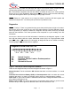
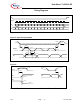
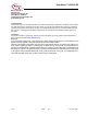
Figure 5: Power Outputs
Timing is valid for resistive load with parallel and serial control.
Rising edge of chip select initiates the switching
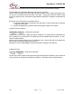
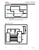
Application Circuits
t
t
t
ON
t
OFF
80%
V
DS
V
IN
20%
OUT1
OUT2
OUT8
TLE
6230 GP
SI
SO
CLK
CS
VS
V
S
= 5V
RESET
GND
V
BB
CLK
MTSR
MRST
P xy
µC
e.g. C167
IN1
IN2
IN3
IN4
PRG
FAULT
10k
C