
Datasheet


Data Sheet TLE 6220 GP
V2.2 Page 2009-11-18
12
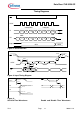
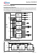
Timing Diagrams
Figure 2: Serial Interface
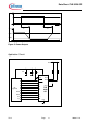
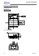
Figure 3: Input Timing Diagram
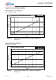
Figure 4:
SO Valid Time Waveforms Enable and Disable Time Waveforms
Data
Bits
6 74444 84444
Control
Bits
6 74444 84444
CS
SCLK
SI
OLD NEW
7 6 5 4 3 2 1 0
SO
7 6 5 4 3 2 1 0
MSB
LSB
Outputs
t
lead
t
SCKH
0.2V
S
t
lag
t
H
t
SCKL
0.2 V
S
t
SU
0.7V
S
0.2V
S
CS
SCLK
SI
0.7VS
t
dt
0.7VS
t
valid
SCLK
CS
SO
t
Dis
0.2 V
S
SO
0.7 V
S
0.7 V
S
0.2 V
S
SO
0.7 V
S
0.2 V
S