
Datasheet

Data Sheet 6 Rev. 1.2, 2008-10-28
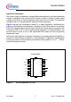
TLE 4473 GV55-2
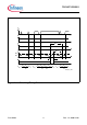
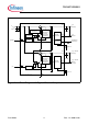
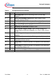
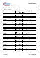
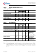
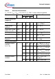
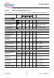
Table 1 Pin Definitions and Functions
Pin No. Symbol Function
1WIWatchdog input; input for watchdog pulses, positive edge
triggered.
2RO1Reset and watchdog output for Q1; open collector output.
Connect to pull-up resistor.
3RO2Reset output 2; open collector output. Connect to pull-up resistor.
4Q2Stand-by regulator output voltage; block to GND with a capacitor
C
Q2
≥ 10 µF, ESR < 5 Ω at 10 kHz.
5N.C.Internally not connected; connect to GND.
6Q1Main regulator output voltage; output voltage tracked to Q2
voltage; block to GND with a capacitor
C
Q1
≥ 10 µF, ESR < 3 Ω at
10 kHz
7I Input voltage; block to ground directly at the IC with a ceramic
capacitor.
8INH1
Inhibit input 1; low level disables Q1, integrated pull-down resistor.
9INH2
Inhibit input 2; low level at INH2 and INH1 disables Q2 and Q1,
integrated pull-down resistor.
10 D1 Reset Delay 1; connect to ground via a capacitor to set reset delay
for Q1.
11 D2 Reset Delay 2; connect to ground via a capacitor to set reset delay
and watchdog timing for Q2.
12 GND Ground; connect to heatslug.
Heatslug Interconnect with PCB heatsink area and GND.