
Datasheet

Data Sheet 12 Rev. 1.2, 2008-10-28
TLE 4473 GV55-2
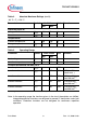
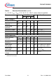
Reset Timing D1
Charge current
I
DC1
4.0 8.0 14.0 µA V
D1
= 1 V
Upper timing
threshold
V
DU1
1.6 1.8 2.2 V –
Lower timing
threshold
V
DL2
0.3 0.4 0.6 V –
Saturation Voltage
V
D1,SAT
––100mVV
Q1
< V
RT1
Reset delay time T
RD1
14 20 30 ms C
D1
= 100 nF
Reset reaction time
T
rr
––10µs C
D1
= 100 nF
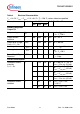
Reset Output RO1
Reset switching
threshold
V
RT1
4.5 4.65 4.8 V –
V
RT1
/V
Q1
90 93 96 % –
Reset threshold
headroom
V
R1HEAD
200 350 500 mV V
Q1
- V
RT1
Reset output
sink current
I
RO1
1.0––mAV
Q1
= 5.0 V; V
Q2
= 5.0 V;
V
D1
= 0 V; V
RO1
= 0.3 V
Reset output
low voltage
V
RO1L
–0.150.3VV
Q1
≥ 1 V
I
RO1
= 1 mA
Reset output high
voltage
V
RO1H
4.5––VR
RO1,ext
= 4.7 kΩ
1) Drop voltage = V
I
- V
Q
(measured when the output voltage has dropped 100 mV from the nominal value
obtained at 13.5 V input)
Table 4 Electrical Characteristics (cont’d)
V
I1
= 13.5 V; V
INH1
= V
INH2
= 5 V; -40 °C < T
j
< 150 °C; unless otherwise specified
Parameter Symbol Limit Values Unit Test Condition
Min. Typ. Max.