
Datasheet
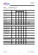

Data Sheet 16 Rev. 1.6, 2009-02-03
TLE 4471
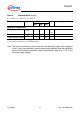
The reset delay time t
dr
is defined by the reset delay capacitor C
DR
at pin DR and can be
calculated as follows:
(1)
Definitions:
•
C
DR
= reset delay capacitor
•
t
dr
= reset delay time required by the application
•
V
DR, dt
= typical 1.8 V for power up reset
•
I
DR, ch
= charge current typical 4 µA
For a delay capacitor
C
DR
= 100 nF the typical power up reset delay time is 45 ms.
The undervoltage reset circuitry supervises the output voltage. In case
V
Q1
falls below
the reset threshold the reset output is set LOW after the reset reaction time
t
rr
(discharge
of the reset delay capacitor). The reset LOW signal is held down to an output voltage
V
Q1
of 1 V. Both, the reset reaction time and the reset delay time are defined by the capacitor
value.
The reset reaction time
t
rr
is the time it takes the voltage regulator to set its reset output
LOW after the output voltage has dropped below the reset threshold. The reset reaction
time can be calculated using the following equation:
(2)
t
rd
C
DR
V
DR dt,
I
DR ch,
---------------
×=
t
rr
C
DR
V
DR dt,
V
DR st,
–
I
DR dis,
------------------------------------
×=