
Datasheet

TLE 4471
Data Sheet 11 Rev. 1.6, 2009-02-03
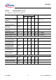
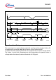
Reset delay charging
current
I
DR, ch
246µA V
DR
= 1 V
Reset delay
discharge current
I
DR, dis
60 120 160 mA V
DR
= 1 V
Upper reset timing
threshold
V
DR, dt
0.91.82.7V –
Lower timing
threshold
V
DR, st
0.25 0.4 0.65 V –
Reset delay time
t
dr
35 50 70 ms C
R
= 100 nF
Reset reaction time
t
rr
0.5 – 3 µs C
R
= 100 nF
Watchdog
Watchdog input
pull-down resistor
R
W
51540kΩ –
Watchdog delay
charging current
I
DW, ch
246µA V
DW
= 1 V; V
DR
= 2.7 V
Watchdog upper
timing threshold
V
DW, dt
1.51.92.5V –
Watchdog lower
timing threshold
V
DW, st
0 30 200 mV –
Watchdog trigger
pulse interval
t
wp
35 50 70 ms C
DW
= 100 nF
Reference Output REF2
Voltage divider ratio
V
REF2
49.5 50 50.5 % of
V
Q2
–
Output impedance
R
REF2
10 – 20 kΩ –
Output clamp voltage – – – 4.5 V –
Table 4 Characteristics (cont’d)
V
I
= 13.5 V; T
j
= -40 °C < T
j
< 125 °C
Parameter Symbol Limit Values Unit Measuring Condition
Min. Typ. Max.