
Datasheet


Datasheet 4 Rev. 1.0, 2007-03-20
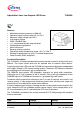
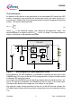
TLE4309
Note: Stresses above the ones listed here may cause permanent damage to the device.
Exposure to absolute maximum rating conditions for extended periods may affect
device reliability.
Note: Integrated protection functions are designed to prevent IC destruction under fault
conditions described in the data sheet. Fault conditions are considered as
“outside” normal operating range. Protection functions are not designed for
continuous repetitive operation.
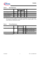
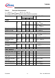
Table 2 Absolute Maximum Ratings
Parameter Symbol Limit Values Unit Remarks
Min. Max.
Input
Voltage
V
I
-42 45 V –
Current
I
I
– – mA internally limited
Output
Voltage
V
Q
-1 40 V –
Current
I
Q
– – mA internally limited
Reference Input
Voltage
V
REF
-1 16 V –
Current
I
REF
-2 2 mA –
Pulse Width Modulation / Enable Input
Voltage
V
PWM
-40 40 V –
Current
I
PWM
-1 1 mA –
Temperatures
Junction temperature
T
j
-40 150 °C–
Storage temperature
T
stg
-50 150 °C–
ESD Susceptibility
ESD Resistivity
V
ESD,HBM
-2 2 kV Human Body Model
1)
1) ESD susceptibility, HBM according to EIA/JESD 22-A114B