
Datasheet


TLE4309
Datasheet 3 Rev. 1.0, 2007-03-20
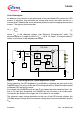
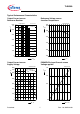
Figure 2 Pin Configuration (top view)
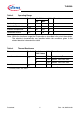
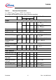
Table 1 Pin Definitions and Functions
Pin No. Symbol Function
1I Input.
2PWM /
EN
Pulse Width Modulation Input / ENABLE input.
If not needed connect to I (pin 1).
3 n. c. Internally not connected. Leave open.
4GNDGround reference; connect to heatsink area and to TAB.
5REFReference Input; connect to shunt resistor.
6 n. c. Internally not connected. Leave open.
7QOutput.
TAB Connect to heatsink area and to GND pin.
TLE4309_PINO UT.VSD
71
P-TO-263
In.cREFQ
PWM
/ EN
GND n.c.
TAB