
Datasheet


Datasheet 2 Rev. 1.0, 2007-03-20
TLE4309
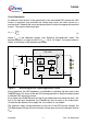
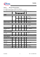
Circuit Description
An external shunt resistor in the ground path of the connected LEDs senses the LED
current. A regulation loop maintains the voltage drop across the shunt resistor at a
constant level. Selecting the shunt resistance permits to adjust the appropriate constant
current . The output current calculates
(1)
where
V
REF
is the reference voltage. (see “Electrical Characteristics” table). The
equation applies in a range of 0.39 Ω ≤
R
REF
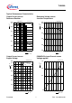
≤ 1.8 Ω. On Page 7, the output current is
shown as a function of the reference resistance.
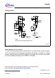
Figure 1 Block Diagram and Typical Application Circuit
During operation, the LED brightness is modifiable by adjusting the duty cycle at the
PWM/EN input. This allows to dim the LEDs during operation or adapt the output current
to different LED luminosity classes.
A low signal at the PWM/EN input sets the IC into sleep mode consuming less than 1 µA.
Due to its high input impedance, the PWM/EN pin can be used as an enable input.
Connect the pin directly to the supply line, if its function is not needed.
The minimum supply voltage calculates as the sum of the LED forward voltages, the
TLE4309 dropout voltage and the maximum voltage drop across the reference resistor
R
REF
.
I
Qtyp,
V
REF
R
REF
------------=
TLE4309_BLOCKDIAGRAM+APPCIRCUIT.VSD
Bandgap
Reference
4
GND
5REF
7
QI
1
PWM
/ EN 2
Temp.
Shutdown
Bias Supply
R
REF
+12V
Logic
op tiona l
100nF
TLE 4309