
Datasheet

Datasheet 6 Rev. 1.1, 2007-10-17
TLE 4299
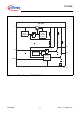
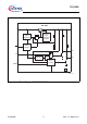
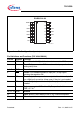
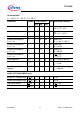
Figure 4 Pin Configuration (top view)
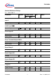
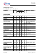
Pin Definitions and Functions (TLE 4299 GMV33)
Pin No. Symbol Function
1RADJReset Threshold Adjust; if not needed connect to GND.
2DReset Delay; connect to GND via external delay capacitor for
setting delay time.
3, 4, 5 GND Ground
6INH
Inhibit: If not needed connect to Input pin I; A high signal
switches the regulator ON.
7ROReset Output; the open-collector output is linked internally to Q
via a 20kΩ pull-up resistor. Keep open, if the pin is not needed.
8SOSense Output; open-collector output. Keep open, if the pin is not
needed.
9QOutput; connect to GND with a 22 µF capacitor, 0.4 Ω <
ESR < 3.7 Ω.
1)
1)
see characteristic curves
10, 11, 12 GND Ground
13 I Input; block to GND directly at the IC by a ceramic capacitor.
14 SI Sense Input; if not needed connect to Q.
AEP02831
141RADJ SI
D2 13
GND 3 12
GND 4 11
10
GND 5
69
INH
RO 7 8
I
GND
GND
GND
Q
SO
PG-DSO-14-30