
Datasheet

TLE42994V33
Pin Configuration
Data Sheet 5 Rev. 1.01, 2010-10-14
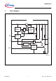
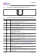
3 Pin Configuration
3.1 Pin Assignment TLE42994GMV33 (PG-DSO-14)
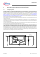
Figure 2 Pin Configuration (top view)
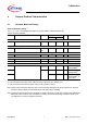
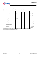
3.2 Pin Definitions and Functions TLE42994GMV33 (PG-DSO-14)
Pin Symbol Function
1
RADJ
Reset Threshold Adjust
connect an external voltage divider to adjust reset threshold;
connect to GND for using internal threshold
2D Reset Delay Timing
connect a ceramic capacitor to GND for adjusting the reset delay time;
leave open if the reset function is not needed
3, 4, 5
GND
Ground
connect all pins to PCB and heatsink area
6EN Enable
high signal enables the regulator;
low signal disables the regulator;
connect to I if the Enable function is not needed
7RO Reset Output
open collector output; internally linked to the output via a 20kΩ pull-up resistor;
leave open if the reset function is not needed
8SO Sense Output
open collector output; internally linked to the output via a 20kΩ pull-up resistor;
leave open if the sense comparator is not needed
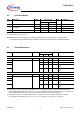
9Q Output
block to GND with a capacitor close to the IC terminals, respecting the values given
for its capacitance C
Q
and ESR in the table “Functional Range” on Page 8
10, 11, 12
GND
Ground
connect all pins to PCB and heatsink area
13 I
Input
for compensating line influences, a capacitor to GND close to the IC terminals is
recommended
14 SI Sense Input
connect the voltage to be monitored;
connect to Q if the sense comparator is not needed
PinConfig_PG-DSO-14.vs
d
SI
I
GND
GND
GND
Q
SO
RADJ
D
GND
GND
GND
EN
RO
14
13
12
11
10
9
8
1
2
3
4
5
6
7