
Datasheet

Data Sheet 18 Rev. 1.01, 2010-10-14
TLE42994V33
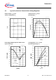
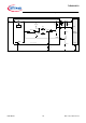
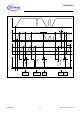
Block Description and Electrical Characteristics
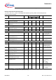
Electrical Characteristics Reset Function
V
I
= 13.5 V, -40 °C ≤ T
j
≤ 150 °C, all voltages with respect to ground, positive current flowing into pin
(unless otherwise specified)
Pos. Parameter Symbol Limit Values Unit Conditions
Min. Typ. Max.
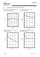
Output Undervoltage Reset
5.6.1 Default Output Undervoltage Reset
Switching Thresholds
V
RT
3.00 3.10 3.20 V V
Q
decreasing
5.6.2 Output Undervoltage Reset
Headroom
V
RH
50 200 300 mV –
Output Undervoltage Reset Threshold Adjustment
5.6.3 Reset Adjust
Switching Threshold
V
RADJ,th
1.26 1.36 1.44 V V
Q
>2.5V
5.6.4 Reset Adjustment Range
1)
1) V
RT
is scaled linearly, in case the Reset Switching Threshold is modified
V
RT,range
2.50 – 3.10 V –
Reset Output RO
5.6.5 Reset Output Low Voltage
V
RO,low
–0.10.4V1V ≤ V
Q
≤ V
RT
no external R
RO,ext
5.6.6 Reset Output Internal
Pull-up Resistor to
V
Q
R
RO
10 20 40 kΩ
–
5.6.7 Optional Reset Output External
Pull-up Resistor to
V
Q
R
RO,ext
5.6––kΩ
1V ≤
V
Q
≤ V
RT
;
V
RO
≤ 0.4 V
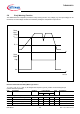
Reset Delay Timing
5.6.8 Delay Pin Output Voltage
V
D
––5V–
5.6.9 Power On Reset Delay Time
t
rd
36 51 60 ms C
D
= 100 nF
Calculated Value:
t
rd
= C
D
* V
DU
/ I
D,ch
5.6.10 Upper Delay
Switching Threshold
V
DU
– 1.85 – V –
5.6.11 Lower Delay
Switching Threshold
V
DL
–0.50–V–
5.6.12 Delay Capacitor
Charge Current
I
D,ch
–3.5–µAV
D
= 1 V
5.6.13 Delay Capacitor
Reset Discharge Current
I
D,dch
– 70 – mA V
D
= 1 V
5.6.14 Delay Capacitor
Discharge Time
t
rr,d
– 1.7 3.0 µs Calculated Value:
t
rr,d
= C
D
*(V
DU
-
V
DL
)/ I
D,dch
C
D
= 100 nF
5.6.15 Internal Reset Reaction Time
t
rr,int
–2025µsC
D
= 0 nF
2)
2) parameter not subject to production test; specified by design
5.6.16 Reset Reaction Time t
rr,total
– 21.7 28 µs Calculated Value:
t
rr,total
= t
rr,int
+ t
rr,d
C
D
= 100 nF