
Datasheet

TLE 4290
Data Sheet 3 Rev. 1.7, 2007-03-20
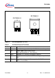
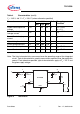
Figure 2 Pin Configuration (top view)
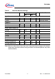
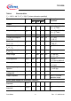
Table 1 Pin Definitions and Functions
Pin No. Symbol Function
1I Input; block to ground directly at the IC with a ceramic capacitor.
2PGPower Good; open collector output.
Add a pull-up resistor of > 5 kΩ to pin Q.
3GNDGround; Pin 3 internally connected to heatsink.
4DDelay; connect a capacitor to GND for setting power good delay
time.
5QOutput; block to ground with a capacitor,
C ≥ 22 μF
ESR < 5 Ω at 10 kHz.
AEP02827
I
PG QDGND
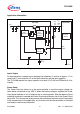
AEP02825
PG D Q
I
GND
PG-TO263-5-1
PG-TO252-5-11