
Datasheet

Data Sheet 10 Rev. 1.7, 2007-03-20
TLE 4290
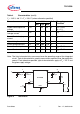
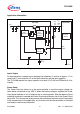
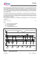
The power good reaction time t
rr
is the time it takes the voltage regulator to set power
good output PG LOW after the output voltage has dropped below the power good
switching threshold. It is typically 0.5 μs for delay capacitor of 47 nF. For other values for
C
D
the reaction time can be estimated using the following equation:
t
rr
= 10 ns/nF × C
D
(2)
The Power Good output is an open collector output. It requires externally a pull-up
resistor of at least 5 kΩ to Q.