
Datasheet

TLE 4270-2
Data Sheet 9 Rev. 1.8, 2007-11-09
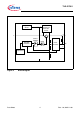
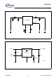
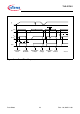
Design Notes for External Components
An input capacitor
C
I
is necessary for compensation of line influences. The resonant
circuit consisting of lead inductance and input capacitance can be damped by a resistor
of approx. 1 Ω in series with
C
I
. An output capacitor C
Q
is necessary for the stability of
the regulating circuit. Stability is guaranteed at values of
C
Q
≥ 22 µF and an ESR of
<3Ω.
Reset Circuitry
If the output voltage decreases below 4.5 V, an external capacitor
C
D
on pin 4 (D) will be
discharged by the reset generator. If the voltage on this capacitor drops below
V
DL
, a
reset signal is generated on pin 2 (RO), i.e. reset output is set low. If the output voltage
rises above the reset threshold,
C
D
will be charged with constant current. After the
power-on-reset time the voltage on the capacitor reaches
V
DU
and the reset output will
be set high again. The value of the power-on-reset time can be set within a wide range
depending of the capacitance of
C
D
.
Reset Timing
The power-on reset delay time is defined by the charging time of an external capacitor
C
D
which can be calculated as follows:
C
D
= (∆t × I
D,c
)/∆V (1)
Definitions:
•
C
D
= delay capacitors
• ∆
t = reset delay time t
rd
• I
D,c
= charge current, typical 14 µA
• ∆
V = V
DU
, typical 1.8 V
V
DU
= upper reset timing threshold at C
D
for reset delay time
t
rd
= ∆V × C
D
/I
D,c
(2)
The reset reaction time
t
rr
is the time it takes the voltage regulator to set the reset out
LOW after the output voltage has dropped below the reset threshold. It is typically 1 µs
for delay capacitor of 47 nF. For other values for
C
D
the reaction time can be estimated
using the following equation:
t
rr
≈ 20 s/F × C
D
(3)