
Datasheet

Data Sheet 2 Rev. 1.8, 2007-11-09
TLE 4270-2
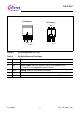
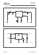
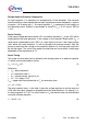
Figure 1 Pin Configuration (top view)
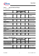
Table 1 Pin Definitions and Functions
Pin Symbol Function
1I Input; block to ground directly at the IC with a ceramic capacitor.
2RO Reset Output; the open collector output is connected to the
5-V output via an integrated resistor of 30 kΩ.
3GNDGround; internally connected to heatsink.
4D Reset Delay; connect a capacitor to ground for delay time adjustment.
5Q 5-V Output; block to ground with 22 µF capacitor, ESR < 3 Ω.
AEP01922
Ι
RO
GND
D
Q
15
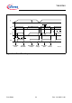
AEP02580
15
ROΙ DQ
GND
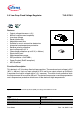
PG-TO263-5-1
PG-TO252-5