
Datasheet


TLE4263-2ES
General Product Characteristics
Data Sheet 6 Rev. 1.0, 2008-04-21
4 General Product Characteristics
4.1 Absolute Maximum Ratings
Note: Stresses above the ones listed here may cause permanent damage to the device. Exposure to absolute
maximum rating conditions for extended periods may affect device reliability.
Note: Integrated protection functions are designed to prevent IC destruction under fault conditions described in the
data sheet. Fault conditions are considered as “outside” normal operating range. Protection functions are
not designed for continuous repetitive operation.
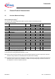
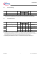
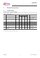
Absolute Maximum Ratings
1)
T
j
= -40 °C to +150 °C; all voltages with respect to ground, positive current flowing into pin
(unless otherwise specified)
1) not subject to production test, specified by design
Pos. Parameter Symbol Limit Values Unit Conditions
Min. Max.
Input I, Input INH
4.1.1 Input Voltage
V
I
, V
INH
-42 45 V –
Reset Output RO, Reset Delay D
4.1.2 Voltage
V
R
, V
D
-0.3 42 V –
Reset Threshold RADJ
4.1.3 Voltage
V
RADJ
-0.3 6 V –
Output Q
4.1.4 Voltage
V
Q
-0.3 7 V –
Watchdog W
4.1.5 Voltage
V
W
-0.3 6 V –
Temperature
4.1.6 Junction Temperature
T
j
–150°C–
4.1.7 Storage Temperature
T
stg
-50 150 °C–
ESD Susceptibility
4.1.8 Human Body Model (HBM)
2)
2) ESD HBM Test according JEDEC JESD22-A114
Voltage - 2 kV –
4.1.9 Charged Device Model (CDM)
3)
3) ESD CDM Test according AEC/ESDA ESD-STM5.3.1-1999
Voltage - 1 kV –