
Datasheet

TLE4253
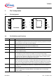
Electrical Characteristics
Data Sheet 8 Rev. 1.2, 2009-11-09
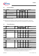
5.1.7 Dropout Voltage
V
dr
= V
I
- V
Q
V
dr
– 280 600 mV I
Q
= 200 mA
2)
5.1.8 Output Current Limitation
I
Q,max
251 400 600 mA V
Q
= (V
ADJ
- 0.1 V);
V
ADJ/EN
= 5 V
5.1.9 Reverse Current
I
Q
-10 -5.5 – mA V
I
= 0 V;
V
Q
= 16 V;
V
ADJ/EN
= 5 V
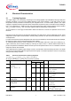
5.1.10 Reverse Current
at Negative Input Voltage
I
I
-5 -2 – mA V
I
= -16 V;
V
Q
= 0 V;
V
ADJ/EN
= 5 V
Feedback Input FB:
5.1.11 Feedback Input Biasing
Current
I
FB
0.1 0.5 µA V
FB
= 5 V
Overtemperature Protection:
5.1.12 Junction Temperature
Equilibrium
T
j,eq
151 – 200 °C T
j
increasing due to power
dissipation generated by the
IC
1)
1) Parameter not subject to production test; specified by design.
2) Measured when the output voltage
V
Q
has dropped 100 mV from its nominal value.
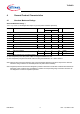
Table 1 Electrical Characteristics Tracking Regulator
V
I
= 13.5 V; V
ADJ/EN
≥ 2.0 V; V
FB
= V
Q
; -40 °C ≤ T
j
≤ 150 °C;
all voltages with respect to ground (unless otherwise specified).
Pos. Parameter Symbol Limit Values Unit Test Condition
Min. Typ. Max.