
Datasheet

TLE4253
Pin Configuration
Data Sheet 4 Rev. 1.2, 2009-11-09
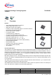
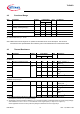
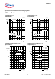
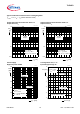
3 Pin Configuration
3.1 Pin Assignment
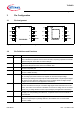
Figure 2 Pin Configuration and Block Diagram
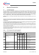
3.2 Pin Definitions and Functions
Pin Symbol Function
1Q Tracker Output.
Block to GND with a capacitor close to the IC terminals, respecting capacitance and ESR
requirements given in the table “Functional Range”.
2, 3, 6, 7 GND Ground reference (version TLE4253GS only).
Interconnect the pins on PCB. Connect to heatsink area.
6GNDGround (version TLE4253E only).
Connect to exposed pad.
2, 3, 7 n. c. Not connected (version TLE4253E only).
Connect to GND externally.
4FBFeedback input for tracker.
Non inverting input of the internal error amplifier to control the output voltage.
Connect this pin directly to the output pin in order to obtain lower or equal output voltages
with respect to the reference voltage and connect a voltage divider for higher output
voltages than the reference (see application information).
5EN/ADJAdjust / Enable.
Connect the reference to this pin. The active high signal of the reference turns on the
device, with active low the tracker is disabled. The reference voltage can be connected
directly or by a voltage divider for lower output voltages (see application information).
8I Input.
IC supply. For compensating line influences, a capacitor close to the IC terminals is
recommended.
–EPExposed pad (version TLE4253E only).
Attach the exposed pad on package bottom to the heatsink area on circuit board.
Connect to GND.
GND
GND
GND
FB EN/ADJ
I
Q
4
3
2
1
TLE4253GS
GND
5
6
7
8
n. c.
n. c.
GND
FB EN/ADJ
I
Q
4
3
2
1
TLE4253E
n. c.
5
6
7
8