
Datasheet


TLE4253
Application Information
Data Sheet 18 Rev. 1.2, 2009-11-09
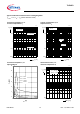
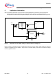
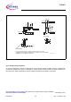
Figure 5 Application circuit: Output voltage
V
Q
higher than reference voltage V
REF
For output voltages higher than the reference voltage, the voltage divider has to be applied between the feedback
and the output according to Figure 5. The equation for the output voltage with respect to the reference voltage is
given by:
Keep in mind that the input voltage has to be at minimum equal to the output voltage plus the dropout voltage of
the regulator.
With a given reference voltage
V
REF
, the desired output voltage V
Q
and the resistor value R1
FB
, the resistor value
for
R2
FB
is given by:
4
ADJ
IFB
Q
EN/
GND
TLE 4253 G
8
2, 3, 6, 7
5
1
µC, e.g. C167
VDD
I/O
Main µC supply, e.g.
TLE4271-2
TLE4278
TLE4470
etc.
IQ
GND
VBAT
VQ > VREF
VREF
R1
FB
R2
FB
V
Q
V
REF
R1
FB
R2
FB
+
R2
FB
---------------------------------
⋅=
R2
FB
R1
FB
V
REF
V
Q
V
REF
–
---------------------------
⋅=