
Datasheet

Data Sheet 8 Rev. 1.0, 2008-05-09
TLE 4252 G
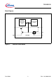
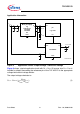
Application Information
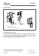
Figure 3 Application Circuit: Output Voltage < Reference Voltage
Figure 3 shows a typical application circuit with
V
Q
< V
REF
. Of course, also V
Q
= V
REF
is
feasible by directly connecting the reference pin of the TLE 4252 D to the appropriate
voltage level without voltage divider.
The output voltage calculates to:
(1)
AEA03535.VSD
Main µC Supply
e.g.
TLE 4271-2
TLE 4278
TLE 4470
etc.
GND
V
BAT
I
Q
R
1ADJ
R
2ADJ
µC
e.g. C167
V
DD
TLE 4252 D
GND
EN
QADJ
I
V
Q
< V
REF
4
1
5
I/O
V
Q
V
REF
R
2ADJ
R
1ADJ
R
2ADJ
+
------------------------------------
×=