
Datasheet

TLE 4252 G
Data Sheet 7 Rev. 1.0, 2008-05-09
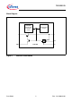
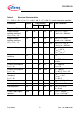
Adjust Input ADJ
Input biasing current
I
ADJ
–0.10.5µA V
ADJ
= 5 V
Enable Input EN
Device on voltage
range
V
EN, on
2.0 – 40 V V
Q
settled
Device off voltage
range
V
EN, off
0–0.8VV
Q
< 0.1 V
Input current
I
EN
-1 2 5 µA V
EN
= 5 V
EN pull-down resistor
R
EN
–1.5–MΩ –
1) Measured when the output voltage V
Q
has dropped 100 mV from the nominal value.
2) The current limit depends also on the input voltage, see graph output current vs. input voltage in the diagrams
section.
3) Specified by design. Not subject to production test.
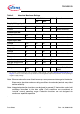
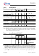
Table 5 Electrical Characteristics (cont’d)
V
I
= 13.5 V; 1.5 V ≤ V
ADJ
≤ V
I
- 0.6 V; -40 °C < T
j
< 150 °C; unless otherwise specified
Parameter Symbol Limit Values Unit Test Condition
Min. Typ. Max.