
Datasheet

TLE 4252 G
Data Sheet 5 Rev. 1.0, 2008-05-09
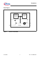
Note: Within the functional range the IC operates as described in the circuit description.
The electrical characteristics are specified within the conditions given in the
related electrical characteristics table.
.
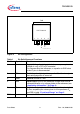
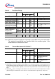
Table 3 Functional Range
Parameter Symbol Limit Values Unit Remarks
Min. Typ. Max.
In- and Output Voltage
Supply voltage V
I
3.5 – 40 V V
I
> V
ADJ
+ V
dr
Enable input voltage V
EN
0–40V–
Adjust input voltage
V
ADJ
1.5 – 40 V –
Error amplifier
common mode range
CMR 1.5 – V
I
-
0.5
V V
Q
≤ V
ADJ
+ ∆V
Q
with
V
FB
= V
Q
Output Capacitor
Output Capacitor’s
Requirement
C
Q
10––µF–
ESR(C
Q
)
––5Ω
1)
Temperature
Junction temperature
T
j
-40 – 150 °C–
1) Relevant ESR value at f = 10 kHz. Not subject to production test; specified by design.
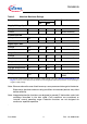
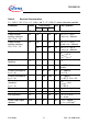
Table 4 Thermal Resistance PG-TO263-5
1)
1) Not subject to production test; specified by design.
Parameter Symbol Limit Values Unit Remarks
Min. Typ. Max.
Junction to case
R
thJC
–4.76K/W–
Junction to ambient
R
thJA
– 24 – K/W 2s2p PCB
2)
2) Specified R
thJA
value is according to Jedec JESD51-2,-5,-7 at natural convection on FR4 2s2p board; The
Product (Chip+Package) was simulated on a 76.2 x 114.3 x 1.5 mm³ board with 2 inner copper layers (2 x
70µm Cu, 2 x 35µm Cu). Where applicable, a thermal via array under the tab contacted the first inner copper
layer.
– 35 – K/W PCB heat sink area
600 mm
2
3)
3) Specified R
thJA
value is according to Jedec JESD 51-3 at natural convection on FR4 1s0p board; The Product
(Chip+Package) was simulated on a 76.2 x 114.3 x 1.5 mm3 board with 1 copper layer (1 x 70 µm Cu).
– 44 – K/W PCB heat sink area
300 mm
2
3)