
Datasheet

TLE 4252 G
Data Sheet 3 Rev. 1.0, 2008-05-09
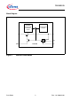
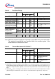
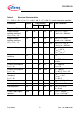
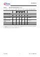
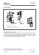
Figure 2 Pin Configuration
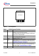
Table 1 Pin Definitions and Functions
Pin No. Symbol Function
1I Supply Voltage Input; Input for battery or a pre-regulated
voltage of a e.g. a DC to DC converter.
For compensating line influences, a capacitor to GND close
to the IC pins is recommended.
2EN Enable Input; a high signal turns on the IC, with a low signal
the tracking regulator is turned off.
3GNDGround; connect to TAB.
4ADJAdjust Input; input for the reference voltage which can be
connected directly or by voltage divider to the reference (see
“Application Information” on Page 8).
5Q Regulator Output; block to GND with a capacitor close to the
IC pins, respecting the values given for its capacitance
C
Q
and ESR in table “Functional Range” on Page 5.
TAB – Connect to GND and heatsink area.
TLE 4252 G_P IN OU T. V S D
1
I
4
ADJ
5
Q
32
EN
TAB
GND
PG-TO-263-5