
Datasheet


Data sheet 3 Rev. 1.0, 2007-07-24
TLE4250-2
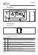
Block Diagram
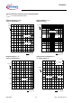
2 Block Diagram
Figure 1 Block Diagram and Simplified Typical Application
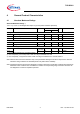
3 Pin Configuration
3.1 Pin Assignment
Figure 2 Pin Configuration Package PG-SCT595-5
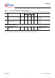
3.2 Pin Definitions and Functions
Pin Symbol Function
1ADJ/ENAdjust / Enable.
Connect the reference to this pin. A low signal disables the IC; a high signal switches it on.
The reference voltage can be connected directly or by a voltage divider for lower output voltages.
For compensating line influences, a capacitor close to the IC pins is recommended.
2GND Ground Reference.
Internally connected to Pin 5. Connect to heatsink area.
3I Input.
IC supply. For compensating line influences, a capacitor close to the IC pins is recommended.
4Q Tracker Output.
Block to GND with a capacitor close to the IC terminals, respecting capacitance and ESR
requirements given in the table “Functional Range”.
5GND Ground Reference.
Internally connected to Pin 2. Connect to heatsink area.
GND
Q
I
B l ockDi agram.vsd
Saturation Control
Current Limitation
Temp.
Protection
C
Q
off-board
load
Supply
C
I
Regulated
Output Voltage
ADJ/EN
Internal
Supply
Reference
TLE 4250-2
ADJ/EN
Volta ge
divider
optional
Pinout.vsd
GND
1
I
5
Q
2
43
GND
ADJ/EN