
Datasheet

SN 7002
Data Sheet 2 05.99
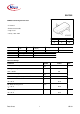
Maximum Ratings
Parameter
Symbol Values Unit
Chip or operating temperature
T
j
-55 ... + 150 ˚C
Storage temperature
T
stg
-55 ... + 150
Thermal resistance, chip to ambient air
R
thJA
≤
350 K/W
Therminal resistance, chip-substrate- reverse side
1)
R
thJSR
≤
285
DIN humidity category, DIN 40 040 E
IEC climatic category, DIN IEC 68-1 55 / 150 / 56
1) For package mounted on aluminium 15 mm x 16.7 mm x 0.7 mm
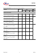
Electrical Characteristics,
at
T
j
= 25˚C, unless otherwise specified
Parameter Symbol Values Unit
min. typ. max.
Static Characteristics
Drain- source breakdown voltage
V
GS
= 0 V,
I
D
= 0.25 mA,
T
j
= 25 ˚C
V
(BR)DSS
60 - -
V
Gate threshold voltage
V
GS
=
V
DS,
I
D
= 1 mA
V
GS(th)
0.8 1.4 2
Zero gate voltage drain current
V
DS
= 60 V,
V
GS
= 0 V,
T
j
= 25 ˚C
V
DS
= 60 V,
V
GS
= 0 V,
T
j
= 125 ˚C
I
DSS
-
-
-
0.1
5
1
µA
Gate-source leakage current
V
GS
= 20 V,
V
DS
= 0 V
I
GSS
- 1 10
nA
Drain-Source on-state resistance
V
GS
= 10 V,
I
D
= 0.5 A
V
GS
= 4.5 V,
I
D
= 0.05 A
R
DS(on)
-
-
3
2
7.5
5
Ω