
Datasheet


C505/C505C/C505A/C505CA
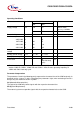
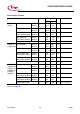
Data Sheet 65 12.00
Note:
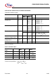
1) V
AIN
may exeed V
AGND
or V
AREF
up to the absolute maximum ratings. However, the conversion result in
these cases will be 00
H
or FF
H
, respectively.
2) During the sample time the input capacitance C
AIN
must be charged/discharged by the external source. The
internal resistance of the analog source must allow the capacitance to reach their final voltage level within t
S
.
After the end of the sample time t
S
, changes of the analog input voltage have no effect on the conversion result.
3) This parameter includes the sample time t
S
, the time for determining the digital result. Values for the
conversion clock t
ADC
depend on programming and can be taken from the table on the previous page.
4) T
UE
(max.) is tested at –40 ≤ T
A
≤= 125 °C ; V
DD
≤ 5.5 V; V
AREF
≤ V
DD
+ 0.1 V and V
SS
= ≤ V
AGND
. It is
guaranteed by design characterization for all other voltages within the defined voltage range.
If an overload condition occurs on maximum 2 unused analog input pins and the absolute sum of input overload
currents on all analog input pins does not exceed 10 mA, an additional conversion error of 1/2 LSB is
permissible.
5) During the conversion the ADC’s capacitance must be repeatedly charged or discharged. The internal
resistance of the reference source must allow the capacitance to reach their final voltage level within the
indicated time. The maximum internal resistance results from the programmed conversion timing.
6) Not 100% tested, but guaranteed by design characterization.