
Datasheet


C505/C505C/C505A/C505CA
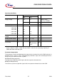
Data Sheet 60 12.00
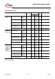
Note:
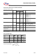
1) Capacitive loading on ports 0 and 2 may cause spurious noise pulses to be superimposed on the V
OL
of ALE
and port 3. The noise is due to external bus capacitance discharging into the port 0 and port 2 pins when these
pins make 1-to-0 transitions during bus operation. In the worst case (capacitive loading > 100 pF), the noise
pulse on ALE line may exceed 0.8 V. In such cases it may be desirable to qualify ALE with a schmitt-trigger,
or use an address latch with a schmitt-trigger strobe input.
2) Capacitive loading on ports 0 and 2 may cause the
V
OH
on ALE and PSEN to momentarily fall below the
0.9
V
DD
specification when the address lines are stabilizing.
3) Overload conditions under operating conditions occur if the voltage on the respective pin exceeds the specified
operating range (i.e.
V
OV
> V
DD
+0.5V or V
OV
< V
SS
- 0.5 V). The absolute sum of input currents on all port
pins may not exceed 50 mA. The supply voltage
V
DD
and V
SS
must remain within the specified limits.
4) Not 100% tested, guaranteed by design characterization.
5) Only valid for C505A-4E and C505CA-4E.
6) Only valid for C505A-4E and C505CA-4E in programming mode.
7)
I
DD
(active mode) is measured with:
XTAL1 driven with
t
R
, t
F
= 5 ns, 50% duty cycle , V
IL
= V
SS
+0.5V, V
IH
= V
DD
– 0.5 V; XTAL2 = N.C.;
EA
=Port 0=RESET=V
DD
; all other pins are disconnected.
8)
I
DD
(idle mode) is measured with all output pins disconnected and with all peripherals disabled;
XTAL1 driven with
t
R
, t
F
= 5 ns, 50% duty cycle, V
IL
= V
SS
+0.5V, V
IH
= V
DD
– 0.5 V; XTAL2 = N.C.;
RESET = EA
= V
SS
; Port0 = V
DD
; all other pins are disconnected; the microcontroller is put into idle mode by
software;
9)
I
DD
(active mode with slow-down mode) is measured with all output pins disconnected and with all peripherals
disabled;
XTAL1 driven with
t
R
, t
F
= 5 ns, 50% duty cycle, V
IL
= V
SS
+0.5V, V
IH
= V
DD
– 0.5 V; XTAL2 = N.C.;
RESET = EA
= V
SS
; all other pins are disconnected; the microcontroller is put into slow-down mode by
software;
10)
I
DD
(idle mode with slow-down mode) is measured with all output pins disconnected and with all peripherals
disabled;
XTAL1 driven with
t
R
, t
F
= 5 ns, 50% duty cycle, V
IL
= V
SS
+0.5V, V
IH
= V
DD
– 0.5 V; XTAL2 = N.C.;
RESET = EA
= V
SS
; Port0 = V
DD
; all other pins are disconnected; the microcontroller is put into idle mode
with slow-down enabled by software;
11)
I
PD
(power-down mode) is measured under following conditions:
Port 0 = E
A = V
DD
; RESET =V
SS
; XTAL2 = N.C.; XTAL1 = V
SS
; V
AGND
= V
SS
; V
AREF
= V
DD
;
all other pins are disconnected.
12) The typical
I
DD
values are periodically measured at T
A
= +25 °C but not 100% tested.
13) The maximum
I
DD
values are measured under worst case conditions (T
A
= 0 °C or -40 °C and V
DD
=5.5V)
14) The values are valid for C505CA-4R, C505CA-2R, C505CA-L, C505A-4R, C505A-2R and C505A-L only.