
Datasheet


C505/C505C/C505A/C505CA
Data Sheet 55 12.00
Lock Bits Programming / Read
The C505A-4E/C505CA-4E has two programmable lock bits which, when programmed according
to Table 13, provide four levels of protection for the on-chip OTP code memory. The state of the
lock bits can also be read.
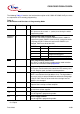
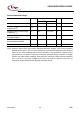
Table 12
Access Modes Selection
Access Mode
EA
/
V
PP
PROG PRD
PMSEL Address
(Port 2)
Data
(Port 0)
10
Program OTP memory byte V
PP
HH H A0-7
A8-14
D0-7
Read OTP memory byte V
IH
H
Program OTP lock bits V
PP
HH L – D1,D0 see
Table 13
Read OTP lock bits V
IH
H
Read OTP version byte V
IH
H L H Byte addr.
of sign. byte
D0-7
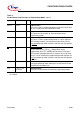
Table 13
Lock Bit Protection Types
Lock Bits at D1,D0 Protection
Level
Protection Type
D1 D0
1 1 Level 0 The OTP lock feature is disabled. During normal operation of
the C505A-4E/C505CA-4E, the state of the EA
pin is not
latched on reset.
1 0 Level 1 During normal operation of the C505A-4E/C505CA-4E, MOVC
instructions executed from external program memory are
disabled from fetching code bytes from internal memory. EA
is
sampled and latched on reset. An OTP memory read operation
is only possible using the ROM/OTP verification mode 2 for
protection level 1. Further programming of the OTP memory is
disabled (reprogramming security).
0 1 Level 2 Same as level 1, but also OTP memory read operation using
OTP verification mode is disabled.
0 0 Level 3 Same as level 2; but additionally external code execution by
setting EA
=low during normal operation of the C505A-4E/
C505CA-4E is no more possible.
External code execution, which is initiated by an internal
program (e.g. by an internal jump instruction above the ROM
boundary), is still possible.