
Datasheet
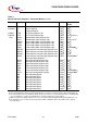
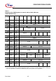
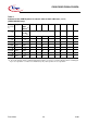

C505/C505C/C505A/C505CA
Data Sheet 20 12.00
Ports P0
P1
P1ANA
2) 4)
P2
P3
P4
Port 0
Port 1
Port 1 Analog Input Selection Register
Port 2
Port 3
Port 4
80
H
1)
90
H
1)
90
H
1)
A0
H
1)
B0
H
1)
E8H
1)
FF
H
FF
H
FF
H
FF
H
FF
H
XXXXXX11
B
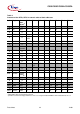
Serial
Channel
ADCON0
2)
PCON
2)
SBUF
SCON
SRELL
SRELH
A/D Converter Control Register 0
Power Control Register
Serial Channel Buffer Register
Serial Channel Control Register
Serial Channel Reload Register, low byte
Serial Channel Reload Register, high byte
D8
H
1)
87
H
99
H
98
H
1)
AA
H
BA
H
00X00000
B
3)
00
H
XX
H
3)
00
H
D9
H
XXXXXX11
B
3)
Timer 0/
Timer 1
TCON
TH0
TH1
TL0
TL1
TMOD
Timer 0/1 Control Register
Timer 0, High Byte
Timer 1, High Byte
Timer 0, Low Byte
Timer 1, Low Byte
Timer Mode Register
88
H
1)
8C
H
8D
H
8A
H
8B
H
89
H
00
H
00
H
00
H
00
H
00
H
00
H
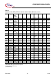
Compare/
Capture
Unit /
Timer 2
CCEN
CCH1
CCH2
CCH3
CCL1
CCL2
CCL3
CRCH
CRCL
TH2
TL2
T2CON
IEN0
2)
IEN1
2)
Comp./Capture Enable Reg.
Comp./Capture Reg. 1, High Byte
Comp./Capture Reg. 2, High Byte
Comp./Capture Reg. 3, High Byte
Comp./Capture Reg. 1, Low Byte
Comp./Capture Reg. 2, Low Byte
Comp./Capture Reg. 3, Low Byte
Reload Register High Byte
Reload Register Low Byte
Timer 2, High Byte
Timer 2, Low Byte
Timer 2 Control Register
Interrupt Enable Register 0
Interrupt Enable Register 1
C1
H
C3
H
C5
H
C7
H
C2
H
C4
H
C6
H
CB
H
CA
H
CD
H
CC
H
C8
H
1)
A8
H
1)
B8
H
1)
00
H
3)
00
H
00
H
00
H
00
H
00
H
00
H
00
H
00
H
00
H
00
H
00X00000
B
3)
00
H
00
H
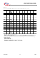
Watchdog WDTREL
IEN0
2)
IEN1
2)
IP0
2)
Watchdog Timer Reload Register
Interrupt Enable Register 0
Interrupt Enable Register 1
Interrupt Priority Register 0
86
H
A8
H
1)
B8
H
1)
A9
H
00
H
00
H
00
H
00
H
Pow. Save
Modes
PCON
2)
PCON1
4)
Power Control Register
Power Control Register 1
87
H
88
H
1)
00
H
0XX0XXXX
B
3)
1) Bit-addressable special function registers
2) This special function register is listed repeatedly since some bits of it also belong to other functional blocks.
3) “X“ means that the value is undefined and the location is reserved
4) SFR is located in the mapped SFR area. For accessing this SFR, bit RMAP in SFR SYSCON must be set.
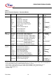
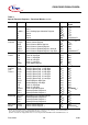
Table 3
Special Function Registers - Functional Blocks (cont’d)
Block Symbol Name Address Contents after
Reset