
Datasheet


C515C
Data Sheet 60 2003-02
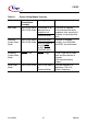
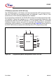
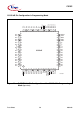
The following Table 12 contains the functional description of all C515C-8E pins which
are required for OTP memory programming.
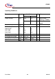
Table 12 Pin Definitions and Functions in Programming Mode
Symbol Pin Number I/O
1)
Function
RESET
1IReset
This input must be at static “0” (active) level during the
whole programming mode.
PMSEL0
PMSEL1
15
16
I
I
Programming mode selection pins
These pins are used to select the different access
modes in programming mode. PMSEL1,0 must satisfy
a setup time to the rising edge of PALE. When the logic
level of PMSEL1,0 is changed, PALE must be at low
level.
PSEL
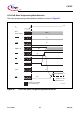
17 I Basic programming mode select
This input is used for the basic programming mode
selection and must be switched according Figure 27.
PRD
18 I Programming mode read strobe
This input is used for read access control for OTP
memory read, version byte read, and lock bit read
operations.
PALE 19 I Programming address latch enable
PALE is used to latch the high address lines. The high
address lines must satisfy a setup and hold time to/from
the falling edge of PALE. PALE must be at low level
whenever the logic level of PMSEL1,0 is changed.
XTAL2 36 I XTAL2
Input to the oscillator amplifier.
XTAL1 37 O XTAL1
Output of the inverting oscillator amplifier.
PMSEL1 PMSEL0 Access Mode
00Reserved
0 1 Read version bytes
1 0 Program/read lock bits
1 1 Program/read OTP memory
byte