
Datasheet


C161S
Timing Characteristics
Data Sheet 62 V1.0, 2003-11
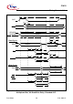
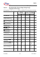
Data float after RdCS
(no RW-delay)
1)
t
68
SR – 0 + t
F
– TCL - 20
+ 2
t
A
+ t
F
1)
ns
Address hold after
RdCS
, WrCS
t
55
CC -6 + t
F
– -6 + t
F
– ns
Data hold after WrCS
t
57
CC 6 + t
F
– TCL - 14
+
t
F
– ns
1) RW-delay and t
A
refer to the next following bus cycle (including an access to an on-chip X-Peripheral).
2) Read data are latched with the same clock edge that triggers the address change and the rising RD
edge.
Therefore address changes before the end of RD
have no impact on read cycles.
3) These parameters refer to the latched chip select signals (CSxL
). The early chip select signals (CSxE) are
specified together with the address and signal BHE
(see figures below).
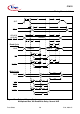
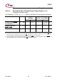
Table 18 Demultiplexed Bus (Standard Supply Voltage Range) (cont’d)
(Operating Conditions apply)
ALE cycle time = 4 TCL + 2
t
A
+ t
C
+ t
F
(80 ns at 25 MHz CPU clock without waitstates)
Parameter Symbol Max. CPU Clock
= 25 MHz
Variable CPU Clock
1 / 2TCL = 1 to 25 MHz
Unit
Min. Max. Min. Max.