
Datasheet

C161S
Timing Characteristics
Data Sheet 52 V1.0, 2003-11
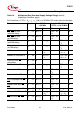
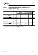
ALE fall. edge to RdCS,
WrCS
(with RW delay)
t
42
CC 16 + t
A
– TCL - 4
+
t
A
– ns
ALE fall. edge to RdCS,
WrCS
(no RW delay)
t
43
CC -4 + t
A
– -4
+
t
A
– ns
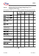
Address float after
RdCS
, WrCS (with RW
delay)
t
44
CC – 0 – 0ns
Address float after
RdCS
, WrCS (no RW
delay)
t
45
CC – 20 – TCL ns
RdCS
to Valid Data In
(with RW delay)
t
46
SR – 16 + t
C
– 2TCL - 24
+
t
C
ns
RdCS
to Valid Data In
(no RW delay)
t
47
SR – 36 + t
C
– 3TCL - 24
+
t
C
ns
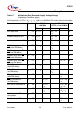
RdCS
, WrCS Low Time
(with RW delay)
t
48
CC 30 + t
C
– 2TCL - 10
+
t
C
– ns
RdCS
, WrCS Low Time
(no RW delay)
t
49
CC 50 + t
C
– 3TCL - 10
+
t
C
– ns
Data valid to WrCS
t
50
CC 26 + t
C
– 2TCL - 14
+
t
C
– ns
Data hold after RdCS
t
51
SR 0 – 0 – ns
Data float after RdCS
t
52
SR – 20 + t
F
– 2TCL - 20
+
t
F
ns
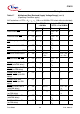
Address hold after
RdCS
, WrCS
t
54
CC 20 + t
F
– 2TCL - 20
+
t
F
– ns
Data hold after WrCS
t
56
CC 20 + t
F
– 2TCL - 20
+
t
F
– ns
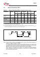
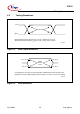
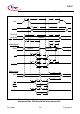
1) These parameters refer to the latched chip select signals (CSxL). The early chip select signals (CSxE) are
specified together with the address and signal BHE
(see figures below).
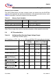
Table 16 Multiplexed Bus (Standard Supply Voltage Range) (cont’d)
(Operating Conditions apply)
ALE cycle time = 6 TCL + 2
t
A
+ t
C
+ t
F
(120 ns at 25 MHz CPU clock without waitstates)
Parameter Symbol Max. CPU Clock
= 25 MHz
Variable CPU Clock
1 / 2TCL = 1 to 25 MHz
Unit
Min. Max. Min. Max.