
Datasheet

C161S
Timing Characteristics
Data Sheet 50 V1.0, 2003-11
Memory Cycle Variables
The timing tables below use three variables which are derived from the BUSCONx
registers and represent the special characteristics of the programmed memory cycle.
Table 15 describes, how these variables are to be computed.
Note: Please respect the maximum operating frequency of the respective derivative.
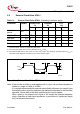
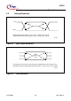
5.4 AC Characteristics
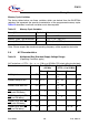
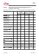
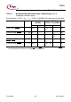
Table 15 Memory Cycle Variables
Description Symbol Values
ALE Extension
t
A
TCL × <ALECTL>
Memory Cycle Time Waitstates
t
C
2TCL × (15 - <MCTC>)
Memory Tristate Time
t
F
2TCL × (1 - <MTTC>)
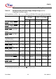
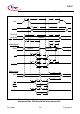
Table 16 Multiplexed Bus (Standard Supply Voltage Range)
(Operating Conditions apply)
ALE cycle time = 6 TCL + 2
t
A
+ t
C
+ t
F
(120 ns at 25 MHz CPU clock without waitstates)
Parameter Symbol Max. CPU Clock
= 25 MHz
Variable CPU Clock
1 / 2TCL = 1 to 25 MHz
Unit
Min. Max. Min. Max.
ALE high time
t
5
CC 10 + t
A
– TCL - 10
+
t
A
– ns
Address setup to ALE
t
6
CC 4 + t
A
– TCL - 16
+
t
A
– ns
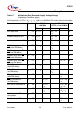
Address hold after ALE
t
7
CC 10 + t
A
– TCL - 10
+
t
A
– ns
ALE falling edge to RD
,
WR
(with RW-delay)
t
8
CC 10 + t
A
– TCL - 10
+
t
A
– ns
ALE falling edge to RD
,
WR
(no RW-delay)
t
9
CC -10 + t
A
– -10 + t
A
– ns
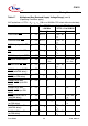
Address float after RD,
WR
(with RW-delay)
t
10
CC – 6 – 6ns
Address float after RD
,
WR
(no RW-delay)
t
11
CC – 26 – TCL + 6 ns