
Datasheet


C161K
C161O
Data Sheet 31 V2.0, 2001-01
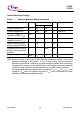
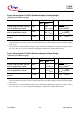
RSTIN active current
4)
I
RSTL
6)
-100 – µA V
IN
= V
IL
RD/WR inact. current
7)
I
RWH
5)
– -40 µA V
OUT
= 2.4 V
RD
/WR active current
7)
I
RWL
6)
-500 – µA V
OUT
= V
OLmax
ALE inactive current
7)
I
ALEL
5)
– 40 µA V
OUT
= V
OLmax
ALE active current
7)
I
ALEH
6)
500 – µA V
OUT
= 2.4 V
Port 6 inactive current
7)
I
P6H
5)
– -40 µA V
OUT
= 2.4 V
Port 6 active current
7)
I
P6L
6)
-500 – µA V
OUT
= V
OL1max
PORT0 configuration current
7)
I
P0H
5)
– -10 µA V
IN
= V
IHmin
I
P0L
6)
-100 – µA V
IN
= V
ILmax
XTAL1 input current I
IL
CC – ±20 µA0 V < V
IN
< V
DD
Pin capacitance
8)
(digital inputs/outputs)
C
IO
CC – 10 pF f = 1 MHz
T
A
= 25 °C
1)
Keeping signal levels within the levels specified in this table, ensures operation without overload conditions.
For signal levels outside these specifications also refer to the specification of the overload current
I
OV
.
2)
Valid in bidirectional reset mode only.
3)
This specification is not valid for outputs which are switched to open drain mode. In this case the respective
output will float and the voltage results from the external circuitry.
4)
These parameters describe the RSTIN pullup, which equals a resistance of ca. 50 to 250 kΩ.
5)
The maximum current may be drawn while the respective signal line remains inactive.
6)
The minimum current must be drawn in order to drive the respective signal line active.
7)
This specification is valid during Reset and during Adapt-mode.
8)
Not 100% tested, guaranteed by design and characterization.
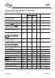
DC Characteristics (Standard Supply Voltage Range) (cont’d)
(Operating Conditions apply)
1)
Parameter Symbol Limit Values Unit Test Condition
min. max.