
Datasheet

Data Sheet 9 Rev 1.0, 2012-09-01
ITS41k0S-ME-N
Application Information
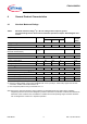
6 Application Information
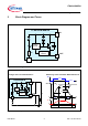
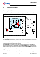
6.1 Application Diagram
The following information is given as a hint for the implementation of the device only and shall not be regarded as
a description or warranty for a certain functionality, condition or quality of the device.
Figure 4 Application Diagram
The ITS41k0S-ME-N can be connected directly to a supply network. It is recommended to place a ceramic
capacitor (e.g.
C
S
= 220nF) between supply and GND to avoid line disturbances. Wire harness inductors/resistors
are sketched in the application circuit above.
The complex load (resistive, capacitive or inductive) must be connected to the output pin OUT.
A built-in current limit protects the device against destruction.
The ITS41k0S-ME-N can be switched on and off with a low power levelshifter switch e.g. Infineon BCR1xx.
The IN pin must be pulled down to GND potential to switch the ITS41k0S-ME-N on. If no current is pulled down,
the IN-node will float up to
V
S
potential by an internal pull up. In this mode the ITS41k0S-ME-N is deactivated with
very low current consumption.
The output voltage slope is controlled during on and off transistion to minimize emissions. Only a small Cercap
C
OUT
=1nF is recommended to attenuate RF noise.
In the following chapters the main features, some typical waverforms and the protection behaviour of the
ITS41k0S-ME-N is shown. For further details please refer to application notes on the Infineon homepage.
complexLOAD
3
ITS41k0S-ME-N
1
Control
Circuit
R
IN
Temperature
Sensor
IN
OUT
V
S
2, 4
Infineon
BCR 1xx
Vctrl
Wire
Harness
complex
LOAD
t
ON
OFF
Electronic Control Unit
Wire
Harness
GND 2
GND 3
C
S
220nF
C
OUT
1nF
GND 1
Vctrl