
Datasheet

Data Sheet 8 Rev 1.0, 2012-09-01
ITS41k0S-ME-N
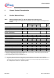
Electrical Characteristics
Standby current I
SOFF
– 2 10 µA IN open 5.0.13
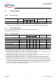
Protection functions
5)
Initial peak short circuit current limit
IN conected to GND
I
LSCP
––1.2AT
j
= -40°C;
V
S
= 13.5V
t
m
= 100µs
5.0.14
Initial peak short circuit current limit
IN conected to GND
I
LSCP
–0.9–AT
j
= 25°C;
V
S
= 13.5V
t
m
= 100µs
5.0.15
Initial peak short circuit current limit
IN conected to GND
I
LSCP
0.2 – – A T
j
=125°C;
V
S
= 13.5V
t
m
= 100µs
5.0.16
Repetitive short circuit current limit
IN conected to GND
I
LSCR
–0.7–A– 5.0.17
Output clamp at
V
OUT
= V
S
- V
DSCL
(inductive load switch off)
V
DSCL
60 – – V I
S
= 4mA 5.0.18
Overvoltage protection
V
SAZ
62 68 – V I
S
= 1mA 5.0.19
Thermal overload
trip temperature
4)
T
jTrip
150 – – °C – 5.0.20
Thermal hysteresis
4)
T
HYS
10 – °C – 5.0.21
Input interface
Off state input current
I
INOFF
– – 0.05 mA T
j
= -25°C;
R
L
= 270Ω;
V
OUT
=< 0.1V
5.0.22
Off state input current
I
INOFF
– – 0.04 mA T
j
= 125°C;
R
L
= 270Ω;
V
OUT
=< 0.1V
5.0.23
On state input current;
IN connected to GND
6)
I
INON
– 0.3 1.0 mA – 5.0.24
Input resistance
R
IN
0.5 1.0 2.5 kΩ – 5.0.25
Reverse Battery
Continuous reverse drain current
I
DREV
– – 0.2 A – 5.0.26
Forward voltage of the drain-source
reverse diode
V
FDS
–600–mVI
FDS
=200mA
I
IN
=< 0.05mA
5.0.27
1) Nominal Load Current is limited by the current limitation; see protection function data
2) Device on 50mm x 50mm x 1,5mm epoxy FR4 PCB with 6cm² (one layer copper 70um thick) copper area for supply voltage
connection. PCB in vertical position without blown air
3) Timing values only with high input slewrates (
t
rIN
= t
fIN
<= 50ns); otherwise slower
4) Not tested in production
5) Integrated protection functions are designed to prevent IC destruction under fault conditions described in the data sheet.
Fault conditions are considered as “outside” normal operating range. Protection functions are not designed for continuous
repetitive operation.
6) Driver circuit must be able to sink currents > 1mA
Table 4 V
S
= 9V to 60V; Tj = -40°C to 125°C; all voltages with respect to ground. Currents flowing into
the device unless otherwise specified in chapter “Block Diagram and Terms”. Typical values
at Vs = 13.5V, Tj = 25°C
Parameter Symbol Values Unit Note /
Test Condition
Number
Min. Typ. Max.