
Datasheet

Data Sheet 7 Rev 1.0, 2012-09-01
ITS41k0S-ME-N
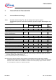
Electrical Characteristics
5 Electrical Characteristics
Table 4 V
S
= 9V to 60V; Tj = -40°C to 125°C; all voltages with respect to ground. Currents flowing into
the device unless otherwise specified in chapter “Block Diagram and Terms”. Typical values
at Vs = 13.5V, Tj = 25°C
Parameter Symbol Values Unit Note /
Test Condition
Number
Min. Typ. Max.
Powerstage
NMOS ON Resistance
R
DSON
–0.81.5Ω I
OUT
= 150mA;
T
j
= 25°C;
IN conected to GND
5.0.1
NMOS ON Resistance
R
DSON
–1.53.0Ω I
OUT
= 150mA;
T
j
= 125°C;
IN conected to GND
5.0.2
NMOS ON Resistance
R
DSON
–25Ω I
OUT
= 50mA;
T
j
= 25°C;
V
S
=6V;
IN conected to GND
5.0.3
Nominal Load Current
1)
;
device on PCB
2)
I
LNOM
0.2 – – A T
a
= 85°C;
T
j
= 125°C;
5.0.4
Timings of Power Stages
Turn ON Time
3)
(to 90% of
V
out
);
V
S
to GND transition of V
IN
t
ON
– – 125
4)
µs V
S
=13.5V;
R
L
= 270Ω
5.0.5
Turn ON Time
3)
(to 90% of
V
out
);
V
S
to GND transition of V
IN
t
ON
–45100µsV
S
=13.5V;
R
L
= 270Ω;
T
j
= 25°C
5.0.6
Turn OFF Time
3)
(to 10% of
V
out
);
GND to
V
S
transition of V
IN
t
OFF
– – 175
4)
µs V
S
=13.5V;
R
L
= 270Ω
5.0.7
Turn OFF Time
3)
(to 10% of
V
out
);
GND to
V
S
transition of V
IN
t
OFF
–40140µsV
S
=13.5V;
R
L
= 270Ω;
T
j
= 25°C
5.0.8
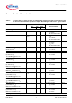
ON-Slew Rate
3)
(10 to 30% of
V
out
);
V
S
to GND transition of V
IN
SR
ON
––6
4)
V / µs V
S
=13.5V;
R
L
= 270Ω
5.0.9
ON-Slew Rate
3)
(10 to 30% of
V
out
);
V
S
to GND transition of V
IN
SR
ON
–1.34.0V / µsV
S
=13.5V;
R
L
= 270Ω;
T
j
= 25°C
5.0.10
OFF-Slew Rate
3)
(70 to 40% of
V
out
);
GND to
V
S
transition of V
IN
SR
OFF
––8
4)
V / µs V
S
=13.5V;
R
L
= 270Ω
5.0.11
OFF-Slew Rate
3)
(70 to 40% of
V
out
);
GND to
V
S
transition of V
IN
SR
OFF
–1.74.0V / µsV
S
=13.5V;
R
L
= 270Ω;
T
j
= 25°C
5.0.12
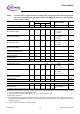
Standby current consumption