
Datasheet

Data Sheet 6 Rev 1.0, 2012-09-01
ITS41k0S-ME-N
General Product Characteristics
4.2 Functional Range
Note: Within the functional range the IC operates as described in the circuit description. The electrical
characteristics are specified within the conditions given in the related electrical characteristics table.
4.3 Thermal Resistance
This thermal data was generated in accordance with JEDEC JESD51 standards.
More information on www.jedec.org.
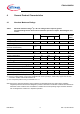
Table 2 Functional Range
Parameter Symbol Values Unit Note /
Test Condition
Number
Min. Typ. Max.
Nominal Operating Voltage
V
S
4.9 – 60 V V
S
increasing 4.2.1
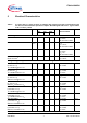
Table 3 Thermal Resistance
1)
1) Not subject to production test, specified by design
Parameter Symbol Values Unit Note /
Test Condition
Number
Min. Typ. Max.
PG-SOT223-4
Junction to Case, Exposed pad
R
thjc
– 40.5 – K/W 4.3.1
Junction to ambient
R
thJA_1s0p
– 145.4 – K/W
2)
2) Specified R
thJA
value is according to Jedec JESD51-3 at natural convection on FR4 1s0p board, footprint; the Product
(Chip+Package) was simulated on a 76.2 x 114.3 x 1.5 mm board with 1x 70µm Cu.
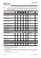
4.3.2
Junction to ambient
R
thJA_1s0p_300mm
–77.2– K/W
3)
3) Specified R
thJA
value is according to Jedec JESD51-3 at natural convection on FR4 1s0p board, Cu, 300mm
2
; the Product
(Chip+Package) was simulated on a 76.2 x 114.3 x 1.5 mm board with 1x 70µm Cu.
4.3.3
Junction to ambient
R
thJA_1s0p_600mm
–66.2– K/W
4)
4) Specified R
thJA
value is according to Jedec JESD51-3 at natural convection on FR4 1s0p board, 600mm
2
; the Product
(Chip+Package) was simulated on a 76.2 x 114.3 x 1.5 mm board with 1x 70µm Cu.
4.3.4
Junction to ambient
R
thJA_2s2p
–57.8– K/W
5)
5) Specified R
thJA
value is according to Jedec JESD51-2,-5,-7 at natural convection on FR4 2s2p board; the Product
(Chip+Package) was simulated on a 76.2 x 114.3 x 1.5 mm board with 2 inner copper layers (2 x 70µm Cu, 2 x 35µm Cu).
4.3.5
Junction to ambient
R
thJA_2s2pvia
–52.9– K/W
6)
6) Specified R
thJA
value is according to Jedec JESD51-2,-5,-7 at natural convection on FR4 2s2p board with two thermal
vias; the Product (Chip+Package) was simulated on a 76.2 x 114.3 x 1.5 mm board with 2 inner copper layers (2 x 70µm
Cu, 2 x 35µm Cu. The diameter of the two vias are equal 0.3mm and have a plating of 25um with a copper heatsink area
of 3mm x 2mm). JEDEC51-7: The two plated-through hole vias should have a solder land of no less than 1.25 mm
diameter with a drill hole of no less than 0.85 mm diameter.
4.3.6