
Datasheet

Data Sheet 5 Rev 1.0, 2012-09-01
ITS41k0S-ME-N
General Product Characteristics
4 General Product Characteristics
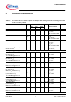
4.1 Absolute Maximum Ratings
Note: Exposure to absolute maximum rating conditions for extended periods may affect device reliability.
Integrated protection functions are designed to prevent IC destruction under fault conditions described in the
data sheet. Fault conditions are considered as “outside” the normal operating range. Protection functions
are not designed for continuous or repetitive operation.
Table 1 Absolute maximum ratings
1)
Tj = 25°C all voltages with respect to ground.
Currents flowing into the device unless otherwise specified in chapter “Block Diagram and
Terms”
1) Not subject to production test, specified by design
Parameter Symbol Values Unit Note /
Test Co
ndition
Min. Typ. Max.
Supply voltage VS
Voltage
V
S
60 V 4.1.1
Output stage OUT
Output Current; (Short circuit current see
electrical characteristics)
I
OUT
self limited A 4.1.2
Input IN
Input Current
I
IN
-15 15 mA 4.1.3
Temperatures
Junction Temperature
T
j
-40 125 °C 4.1.4
Storage Temperature
T
stg
-55 125 °C 4.1.5
Power dissipation
Ta = 25 °C
2)
2) Device on 50mm*50mm*1.5mm epoxy PCB FR4 with 6 cm2 (one layer, 70mm thick) copper area for Vbb
connection. PCB is vertical without blown air
P
tot
1.7 W 4.1.6
Inductive load switch-off energy dissipation
Tj = 150 °C; IL=0.15A; single pulse
1)
E
AS
1000 mJ 4.1.7
ESD Susceptibility
ESD susceptibility (input pin)
V
ESD
-1 1 kV HBM
3)
3) ESD susceptibility HBM according to EIA/JESD 22-A 114.
4.1.8
ESD susceptibility (all other pins)
V
ESD
-5 5 kV HBM
3)
4.1.9